Metal nano optical antenna monolithically integrated on photoelectric detector

A photodetector and metal nanotechnology, which is applied in the field of photodetectors, can solve the problems of high cost and inability to produce in large quantities, and achieve the effects of compact structure, improved quantum efficiency, and simple preparation process

Pending Publication Date: 2018-08-24
SHANGHAI INST OF TECHNICAL PHYSICS - CHINESE ACAD OF SCI
View PDF4 Cites 2 Cited by
  • Summary
  • Abstract
  • Description
  • Claims
  • Application Information

AI Technical Summary

Problems solved by technology

[0004] However, these optical antenna structures are prepared by electron beam lithograph

Method used


Image

  • Metal nano optical antenna monolithically integrated on photoelectric detector
  • Metal nano optical antenna monolithically integrated on photoelectric detector
  • Metal nano optical antenna monolithically integrated on photoelectric detector

Examples


Embodiment 1

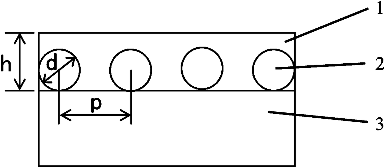
[0022] see figure 1 , as the anti-reflection layer of the InGaAs infrared detector, the substrate 3 is InP, the incident light is 1-1.7 microns, and the incident angle is 0 degrees. Low refractive index cladding layer 1 is SiO 2 , whose thickness is 400 nm. The metal nano-optical antenna material is silver, the diameter is 300 nanometers, and the period is 700 nanometers.

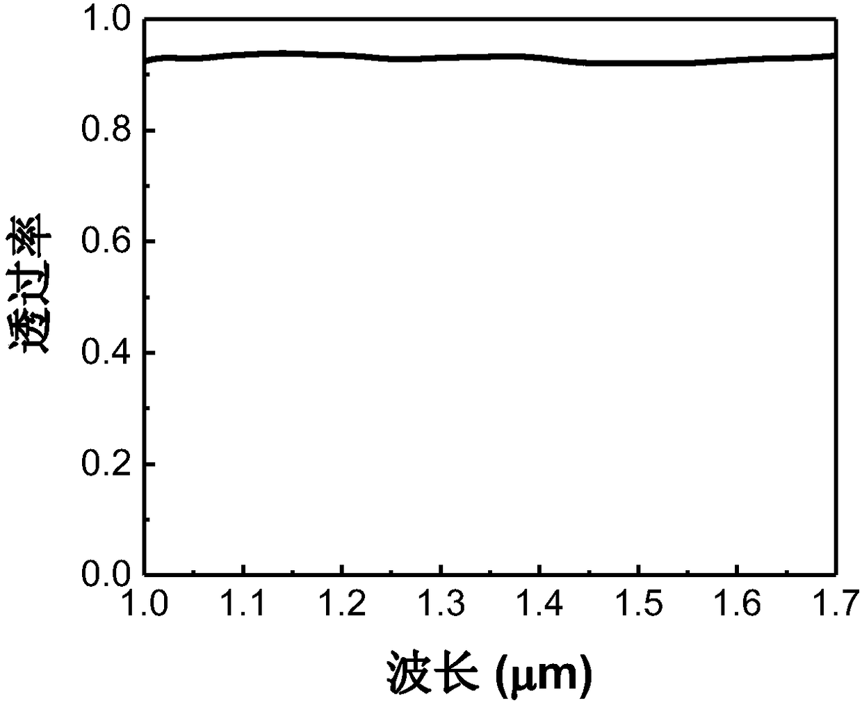
[0023] Under this condition, the relationship between short-wave infrared transmittance and incident wavelength is as follows figure 2 shown. At a wavelength of 1.6 μm, the transmittance is 92%.

Embodiment 2

[0025] see figure 1 , as the anti-reflection layer of the InGaAs infrared detector, the substrate 3 is InP, the incident light is 1-1.7 microns, and the incident angle is 0 degrees. The low refractive index cladding layer 1 is Si 3 N 4 , whose thickness is 500 nm. The metal nano-optical antenna material is gold, the diameter is 400 nanometers, and the period is 800 nanometers.

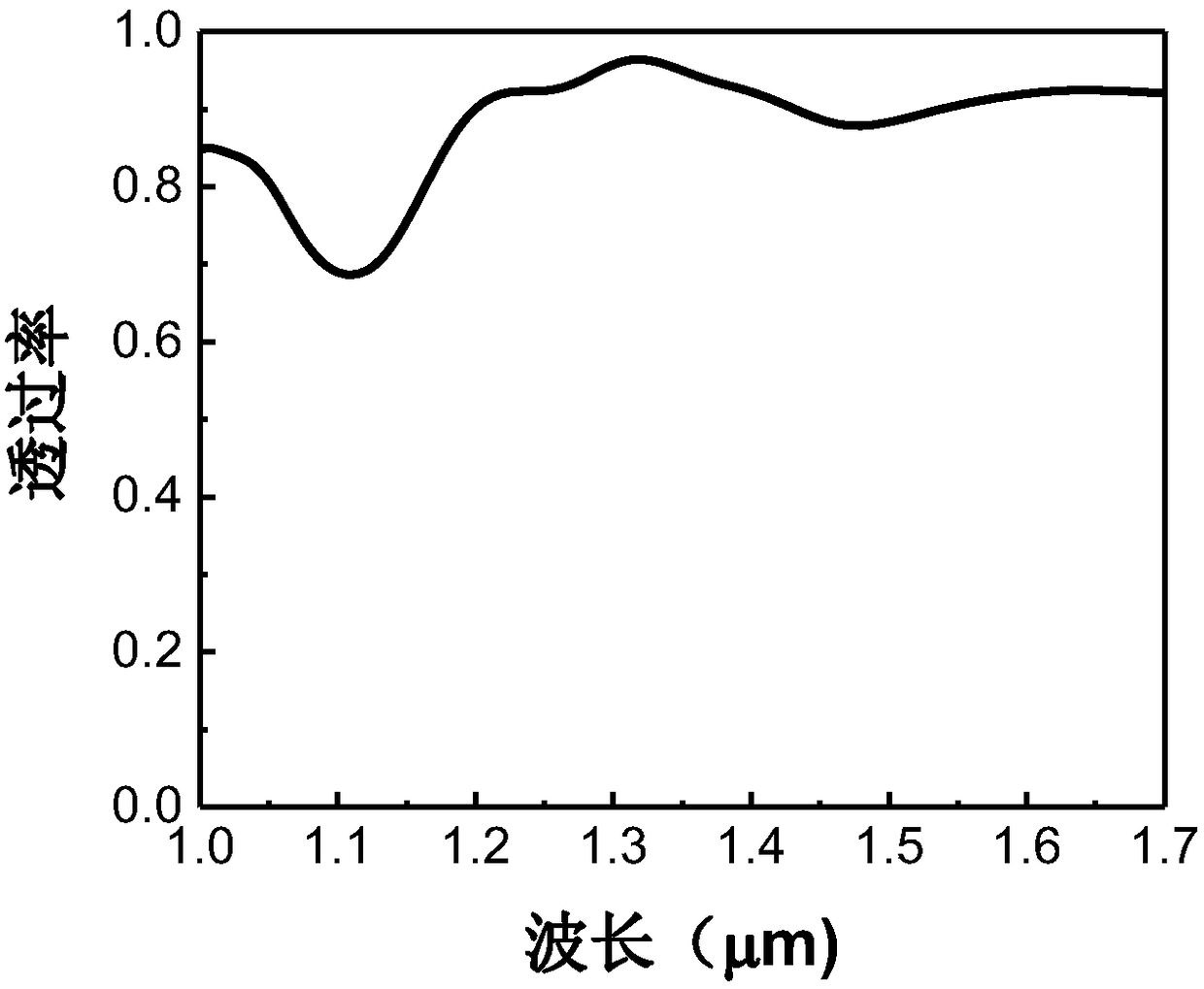
[0026] Under this condition, the relationship between short-wave infrared transmittance and incident wavelength is as follows image 3 shown. At a wavelength of 1.6 μm, the transmittance is 90%.

Embodiment 3

[0028] see figure 1 , as the anti-reflection layer of the InGaAs infrared detector, the substrate 3 is InP, the incident light is 1-1.7 microns, and the incident angle is 0 degrees. The low-refractive-index cladding layer 1 is ZnS, and its thickness is 600 nm. The metal nano-optical antenna material is aluminum, the diameter is 500 nanometers, and the period is 900 nanometers.

[0029] Under this condition, the relationship between short-wave infrared transmittance and incident wavelength is as follows Figure 4 shown. At a wavelength of 1.6 μm, the transmittance is 92%.


PUM

PropertyMeasurementUnit
Diameteraaaaaaaaaa
Thicknessaaaaaaaaaa
Thicknessaaaaaaaaaa

Abstract

The present invention discloses a metal nano optical antenna monolithically integrated on a photoelectric detector. The antenna comprises a covering layer with a low refractive index, a metal nano sphere array and a detector substrate in order from top to bottom. The low refractive index of the covering layer with the low refractive index is in a range of 1.3-2.3, the diameter of each metal nano sphere is 300-500 nanometers, and an arrangement cycle is 700-900 nanometers. The metal nano optical antenna structure can improve the optical absorption properties of the detector, can enhance the response of the detector to an incident light and can improve quantum efficiency through light scattering and surface local field enhancement effect, the preparation process is simple, and the preparation cost is low.

Description

technical field [0001] The invention belongs to the field of photodetectors, in particular to a metal nano-optical antenna monolithically integrated on a photodetector substrate. Background technique [0002] Optical Antenna is a device that can effectively couple the energy radiated in free space to the sub-wavelength scale. Metal nano-optical antennas are generally metal / dielectric structures composed of nano-scale metal particles (spherical, triangular, rod-like and other shapes). The metal surface forms a field enhancement, and at the gap of the antenna, the electric field is greatly enhanced due to the coupling effect. In recent years, nano-optical antennas have attracted the attention of many researchers, showing potential application prospects in many fields such as nano-optical imaging, near-field optical microscope probes, data storage, solar cells, and new light sources. [0003] Chi-Yang Chang et al. found that a 100-nanometer-thick Ag metal film was deposited o...

Claims


Application Information

Patent Timeline
IPC IPC(8): G02B5/00G02B6/122
CPCG02B5/008G02B6/122
Inventor 姚鹏飞李淘李雪邵秀梅龚海梅
Owner SHANGHAI INST OF TECHNICAL PHYSICS - CHINESE ACAD OF SCI
Why Eureka
Try Eureka