Solar cell manufacturing process

A technology of solar cells and manufacturing processes, applied in sustainable manufacturing/processing, final product manufacturing, circuits, etc., can solve the problems of wafer quality decline, waste of processing materials, low rolling efficiency, etc., to achieve uniform density and high adjustment The effect of processing efficiency

Active Publication Date: 2018-08-24
ANHUI HUATENG AGRI TECH CO LTD
View PDF4 Cites 0 Cited by
  • Summary
  • Abstract
  • Description
  • Claims
  • Application Information

AI Technical Summary

Problems solved by technology

[0004] The method of increasing the wafer density of this technical solution realizes extrusion molding of the wafer and increases the wafer density, but this technical solution will roll the material on the upper surface of the wafer to one side, resulting in a higher processing wafer density. Unevenness directly leads to a decline in wafer quality; there are wafers spilling residue on the edge of the mold cavity, which wastes processing materials; intermittent rolling of wafers results in low rolling efficiency

Method used


Image

  • Solar cell manufacturing process
  • Solar cell manufacturing process
  • Solar cell manufacturing process

Examples


Embodiment Construction

[0030] In order to make the technical means, creative features, goals and effects achieved by the present invention easy to understand, the present invention will be further described below in conjunction with specific embodiments.

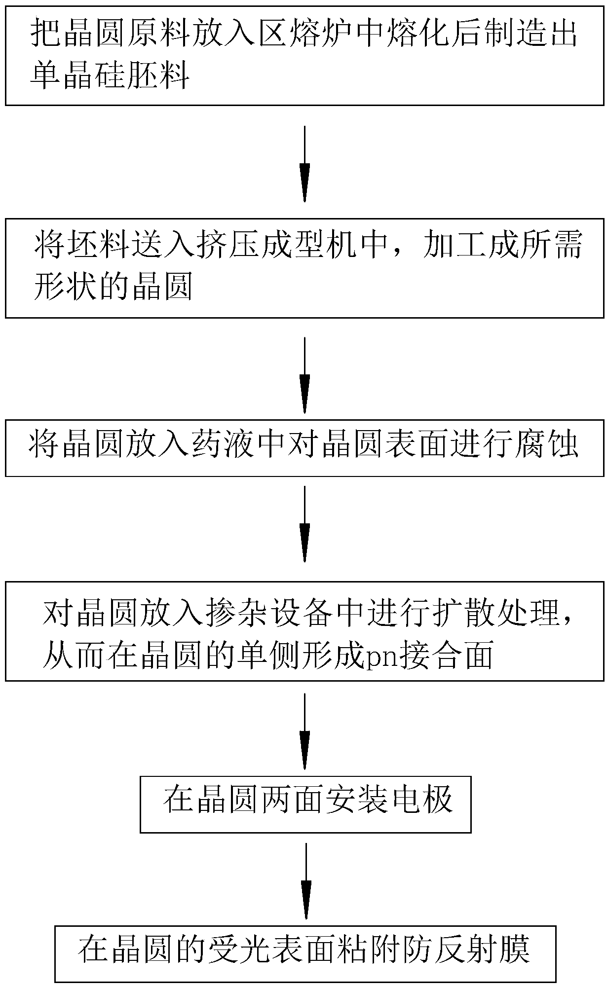
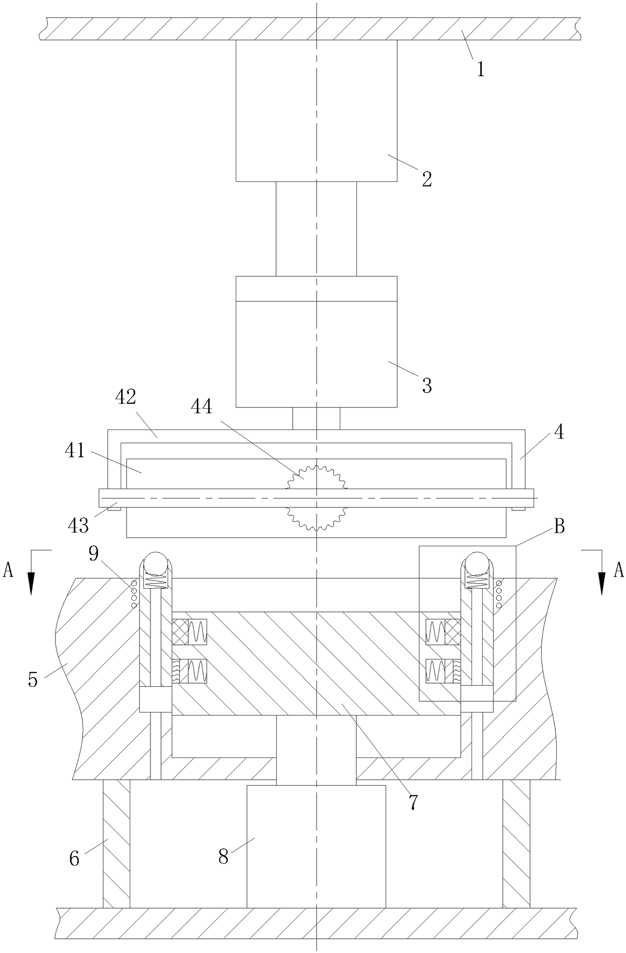
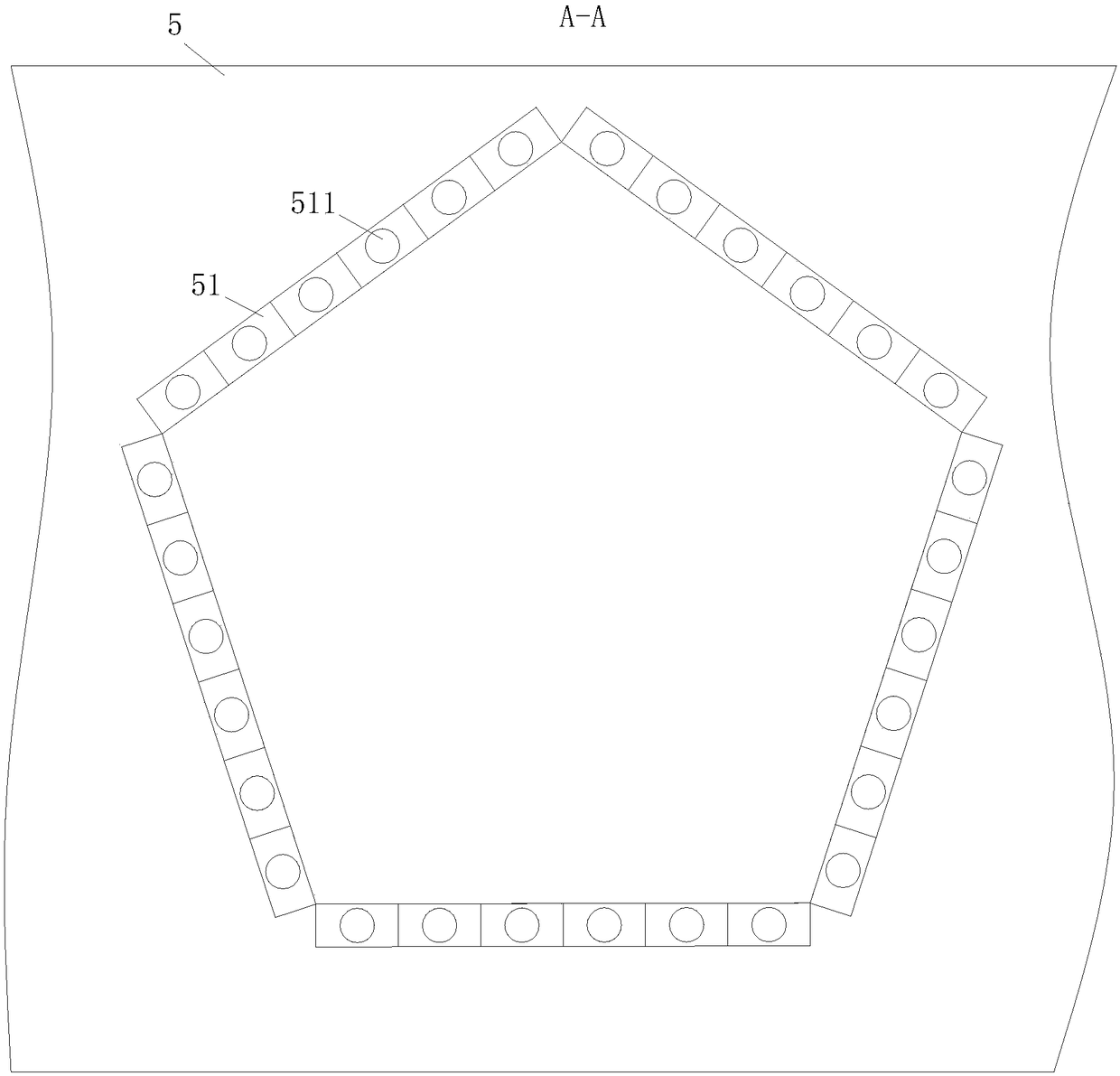
[0031] Such as Figure 1 to Figure 5 Shown, a kind of solar cell manufacturing process of the present invention, this process comprises the steps:

[0032] Step 1: Put the wafer raw material into the zone melting furnace and melt it to produce monocrystalline silicon blank;

[0033] Step 2: Send the blank in step 1 into the extrusion molding machine, and process it into a wafer of the desired shape;

[0034] Step 3: put the wafer in step 2 into the chemical solution to corrode the surface of the wafer;

[0035]Step 4: Put the wafer in step 3 into a doping device for diffusion treatment, so as to form a pn joint surface on one side of the wafer;

[0036] Step 5: Install electrodes on both sides of the wafer in step 4;

[0037] Step 6: Adhering ...


PUM


Abstract

The invention belongs to the technical field of solar cell manufacturing and particularly relates to a solar cell manufacturing process. The process comprises the following steps: a wafer raw materialis put in a zone melting furnace for being melted to manufacture a monocrystalline silicon blank; the blank is fed to an extrusion molding machine to be processed to a wafer in a needed shape; the wafer is put in medicinal liquid to corrode the surface of the wafer; the wafer is put in a doping device for diffusion treatment, and a pn joint surface is thus formed at the single side of the wafer;electrodes are arranged on two sides of the wafer; and an antireflective film is attached to a light receiving surface of the wafer. A motor-driven pressure roller is driven by an electric cylinder, accumulation of materials in the process of rolling does not happen to the wafer, and the density of the rolled wafer is ensured to be uniform; and through arranging a telescopic plate on the peripheryof the side wall of a mold cavity, the melted wafer can be continuously rolled after being lifted at one time by a lifting part, and the wafer processing efficiency is improved.

Description

technical field [0001] The invention belongs to the technical field of solar cell manufacturing, in particular to a solar cell manufacturing process. Background technique [0002] Wafer refers to the silicon chip used in the production of silicon semiconductor integrated circuits. Wafer is the carrier used in the production of integrated circuits. In general, wafers refer to single crystal silicon wafers. Wafer is the most commonly used semiconductor material. According to its diameter, it is divided into 4 inches, 5 inches, 6 inches, 8 inches and other specifications. Recently, 12 inches or even larger specifications have been developed. The larger the wafer, the more ICs that can be produced on the same wafer, which can reduce costs; but the requirements for material technology and production technology are higher, such as uniformity and so on. It is generally believed that the larger the diameter of the silicon wafer, it means that the fab has better technology. In the p...

Claims


Application Information

Patent Timeline
IPC IPC(8): H01L31/18
CPCH01L31/18Y02P70/50
Inventor 王青江振
Owner ANHUI HUATENG AGRI TECH CO LTD
Why Eureka
Try Eureka