Color cadmium-telluride thin-film solar cell and preparation method thereof
A technology of solar cells and cadmium telluride is applied in the field of solar cells to achieve the effects of rich and diverse colors, meeting the needs of building exterior colors, and low cost
- Summary
- Abstract
- Description
- Claims
- Application Information
AI Technical Summary
Problems solved by technology
Method used
Image
Examples
Embodiment 1
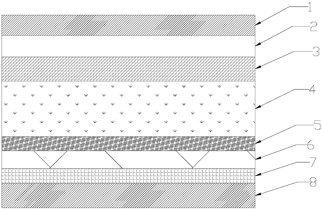
[0041] A preparation method for a colored cadmium telluride thin film solar cell, comprising the following steps:
[0042] (1) Prepare the glass substrate: adopt ordinary float glass as the raw material of the glass substrate, and use PVD to plate metal gold on the ordinary float glass to form a color layer, and the thickness of the color layer is 100nm;
[0043] (2) Deposit fluorine-doped tin oxide on the glass substrate by chemical vapor deposition or magnetron sputtering to form a transparent conductive film;
[0044] Depositing a cadmium sulfide layer on the transparent conductive film layer by magnetron sputtering or chemical water bath method to form a window layer;
[0045] Depositing cadmium telluride on the window layer by magnetron sputtering or evaporation to form an absorber layer;
[0046] Depositing zinc telluride on the absorber layer by magnetron sputtering to form a back contact layer;
[0047] Depositing metallic nickel on the back contact layer by magnetro...
Embodiment 2
[0050] A preparation method for a colored cadmium telluride thin film solar cell, comprising the following steps:
[0051] (1) Prepare the glass substrate: use ultra-white glass as the raw material of the glass substrate, and use CVD to coat the metal compound cerium oxide on the ultra-white glass to form a color layer. The thickness of the color layer is 150nm;
[0052] (2) Deposit fluorine-doped tin oxide on the glass substrate by chemical vapor deposition or magnetron sputtering to form a transparent conductive film;
[0053] Depositing a cadmium sulfide layer on the transparent conductive film layer by magnetron sputtering or chemical water bath method to form a window layer;
[0054] Depositing cadmium telluride on the window layer by magnetron sputtering or evaporation to form an absorber layer;
[0055] Copper chloride is deposited on the absorber layer by magnetron sputtering to form a back contact layer;
[0056]Depositing metal molybdenum on the back contact layer ...
Embodiment 3
[0059] A preparation method for a colored cadmium telluride thin film solar cell, comprising the following steps:
[0060] (1) Prepare the glass substrate: adopt toughened glass as the raw material of the glass substrate, and plate the metal compound copper chloride on the toughened glass by screen printing to form a color layer, the thickness of the color layer is 300nm;
[0061] (2) Deposit fluorine-doped tin oxide on the glass substrate by chemical vapor deposition or magnetron sputtering to form a transparent conductive film;
[0062] Depositing a cadmium sulfide layer on the transparent conductive film layer by magnetron sputtering or chemical water bath method to form a window layer;
[0063] Depositing cadmium telluride on the window layer by magnetron sputtering or evaporation to form an absorber layer;
[0064] Copper chloride is deposited on the absorber layer by magnetron sputtering to form a back contact layer;
[0065] Depositing metallic nickel on the back cont...
PUM
| Property | Measurement | Unit |
|---|---|---|
| Thickness | aaaaa | aaaaa |
Abstract
Description
Claims
Application Information
 - R&D
- Intellectual Property
- Life Sciences
- Materials
- Tech Scout
- Unparalleled Data Quality
- Higher Quality Content
- 60% Fewer Hallucinations
Browse by: Latest US Patents, China's latest patents, Technical Efficacy Thesaurus, Application Domain, Technology Topic, Popular Technical Reports.
© 2025 PatSnap. All rights reserved.Legal|Privacy policy|Modern Slavery Act Transparency Statement|Sitemap|About US| Contact US: help@patsnap.com

