Controllable and perpendicular bismuth selenide nanosheet thin film and preparation method thereof

A technology of nanosheets and thin films, applied in the fields of photodetection and electronic materials

Inactive Publication Date: 2018-09-04
INST OF METAL RESEARCH - CHINESE ACAD OF SCI
View PDF2 Cites 6 Cited by
  • Summary
  • Abstract
  • Description
  • Claims
  • Application Information

AI Technical Summary

Problems solved by technology

[0004] At present, the controllable preparation of vertically grown nanosheets formed by the use of chemical vapor deposition 2 Se 3 Thin films and their photoelectric response properties have not been reported

Method used


Image

  • Controllable and perpendicular bismuth selenide nanosheet thin film and preparation method thereof
  • Controllable and perpendicular bismuth selenide nanosheet thin film and preparation method thereof
  • Controllable and perpendicular bismuth selenide nanosheet thin film and preparation method thereof

Examples


Embodiment 1

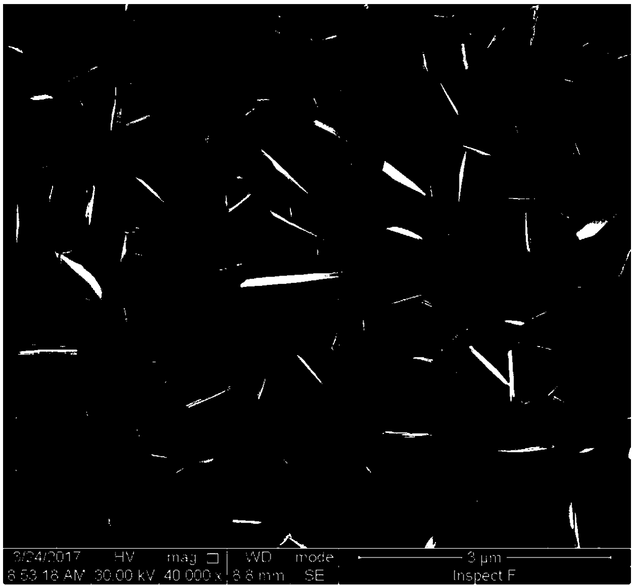
[0041] Preparation of Bi by chemical vapor deposition 2 Se 3 The thin film adopts a P-type silicon substrate as the substrate, and the substrate is cleaned by ultrasound for 5 minutes in ethanol and acetone, and soaked in hydrofluoric acid solution (concentration is 15%) for 1 minute to remove the SiO on the surface. 2 natural oxide layer. The raw material is Bi 2 Se 3 The powder, with a purity of 99.99%, is placed 2 cm upstream from the center of the furnace tube. Before heating, the vacuum in the furnace tube is 0.2Pa, the distance between the substrate and the center of the furnace is 14.5 cm, the total gas flow rate is 50 sccm, the working gas is argon and hydrogen (ratio 4:1), the working pressure is 50 Pa, and the furnace center temperature is 520 °C. Time 3 minutes, Bi 2 Se 3 Thin film scanning electron microscope pictures such as figure 1 shown. Bi 2 Se 3 The current-voltage curves of the PN junction material formed by the thin film and the silicon substrate ...

Embodiment 2

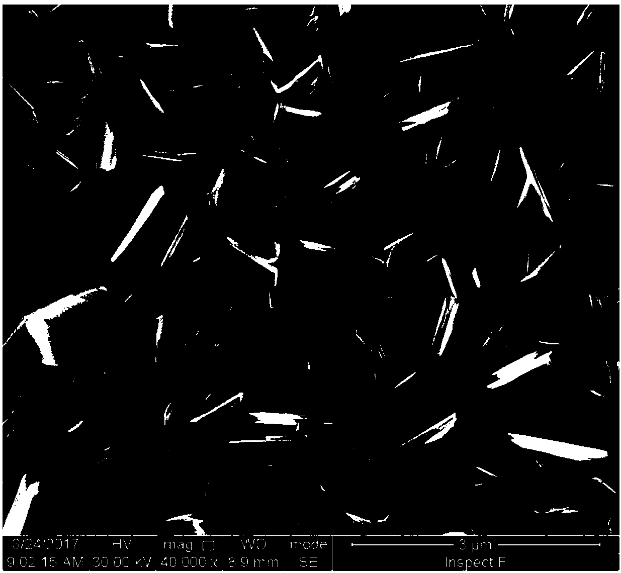
[0043] Preparation of Bi by chemical vapor deposition 2 Se 3 The thin film adopts a P-type silicon substrate as the substrate, and the substrate is cleaned by ultrasound for 5 minutes in ethanol and acetone, and soaked in hydrofluoric acid solution (concentration is 15%) for 1 minute to remove the SiO on the surface. 2 natural oxide layer. The raw material is Bi 2 Se 3 The powder, with a purity of 99.99%, is placed 2 cm upstream from the center of the furnace tube. The distance between the substrate and the center of the furnace is 14.5 cm, the total gas flow rate is 50 sccm, the working gas is argon and hydrogen (ratio 4:1), the working pressure is 50 Pa, the temperature in the center of the furnace is 520 ° C, the working time is 4 minutes, Bi 2 Se 3 Thin film scanning electron microscope pictures such as figure 2 shown. Bi 2 Se 3 The optical test result of the PN junction material formed by the thin film and the silicon substrate is similar to that of Example 3. ...

Embodiment 3

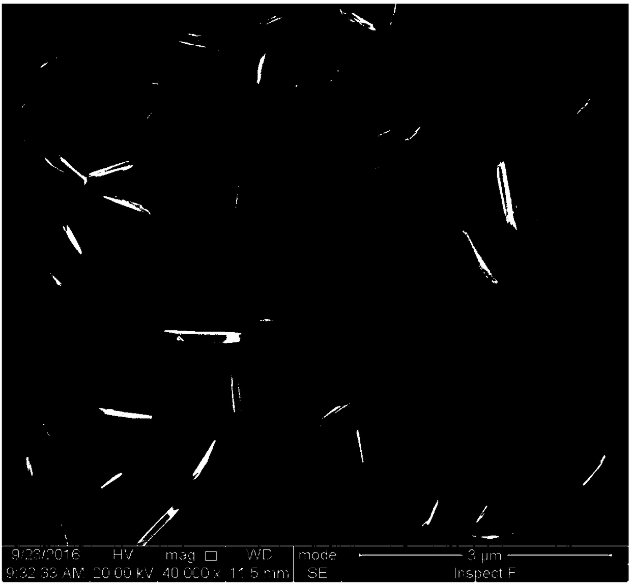
[0045] Preparation of Bi by chemical vapor deposition 2 Se 3 The thin film adopts a P-type silicon substrate as the substrate, and the substrate is cleaned by ultrasound for 5 minutes in ethanol and acetone, and soaked in hydrofluoric acid solution (concentration is 15%) for 1 minute to remove the SiO on the surface. 2 natural oxide layer. The raw material is Bi 2 Se 3 The powder, with a purity of 99.99%, is placed 2 cm upstream from the center of the furnace tube. The distance between the substrate and the center of the furnace is 14.5 cm, the total gas flow rate is 50 sccm, the working gas is argon and hydrogen (ratio 4:1), the working pressure is 50 Pa, the temperature in the center of the furnace is 520 ° C, the working time is 5 minutes, Bi 2 Se 3 Thin film scanning electron microscope pictures such as image 3 As shown, the X-ray diffraction pattern is as Figure 16 As shown, Bi 2 Se 3 The current-voltage curves of the PN junction material formed by the thin fil...


PUM

PropertyMeasurementUnit
sizeaaaaaaaaaa
thicknessaaaaaaaaaa

Abstract

The invention aims to provide a controllable and perpendicular bismuth selenide nanosheet thin film. The thin film comprises Bi2Se3 nanosheets perpendicular to a matrix, wherein the sizes of the nanosheets are 50 nanometers to 50 micrometers. The Bi2Se3 thin film is prepared by a chemical vapor deposition method. By the method, the high-quality thin film having obvious photoelectric response can be controllably prepared, it is found out that the thin film has N-type conductive characteristic by test, the thin film and a P-type silicon substrate can form an N-type thin film/P-type silicon waferdual-layer structure, and the thin film has obvious visible light and near-infrared light photoelectric response capability and relatively rapid photoelectric response time, particularly has high photoresponse capability at a near-infrared wave band and has favorable electric detection application prospect.

Description

technical field [0001] The invention relates to the fields of photoelectric detection and electronic materials, and in particular provides a vertical Bi with controllable morphology 2 Se 3 Thin films composed of nanosheets have obvious photoresponse for visible and near-infrared light detection. Background technique [0002] The principle of a photodetector is that radiation causes a change in the conductivity of the irradiated material. Photoelectric detectors are widely used in various fields of military and national economy, and are mainly used for ray measurement and detection, industrial automatic control, photometric measurement, etc. in the visible or near-infrared band. In 1873, British Smith discovered the photoconductive effect of selenium, but this effect has been in the stage of exploration and research for a long time and has not been practically applied. After the Second World War, with the development of semiconductors, various new photoconductive materials...

Claims


Application Information

Patent Timeline
Patent Type & Authority Applications(China)
IPC IPC(8): H01L31/0328H01L31/18C23C16/02C23C16/30
CPCC23C16/0227C23C16/305H01L31/0328H01L31/18Y02P70/50
Inventor 王振华李名泽张志东高翾
Owner INST OF METAL RESEARCH - CHINESE ACAD OF SCI
Why Eureka
Try Eureka