Thin film heterostructure preparation method

A heterogeneous structure and thin film technology, applied in electrical components, piezoelectric/electrostrictive/magnetostrictive devices, circuits, etc., can solve problems such as inability to perform high-temperature processes, and prevent wafers from automatically peeling off and scratching the surface, The effect of reducing the annealing temperature and avoiding wafer fragmentation

Active Publication Date: 2018-09-04
上海新硅聚合半导体有限公司
View PDF9 Cites 25 Cited by
  • Summary
  • Abstract
  • Description
  • Claims
  • Application Information

AI Technical Summary

Problems solved by technology

[0007] In view of the above-mentioned shortcomings of the prior art, the purpose of the present invention is to provide a method for preparing a thin-film heterogeneous structure, which is used to solve the problem of the thermal strain of the

Method used


Image

  • Thin film heterostructure preparation method
  • Thin film heterostructure preparation method
  • Thin film heterostructure preparation method

Examples


Embodiment Construction

[0048]Embodiments of the present invention are described below through specific examples, and those skilled in the art can easily understand other advantages and effects of the present invention from the content disclosed in this specification. The present invention can also be implemented or applied through other different specific implementation modes, and various modifications or changes can be made to the details in this specification based on different viewpoints and applications without departing from the spirit of the present invention.

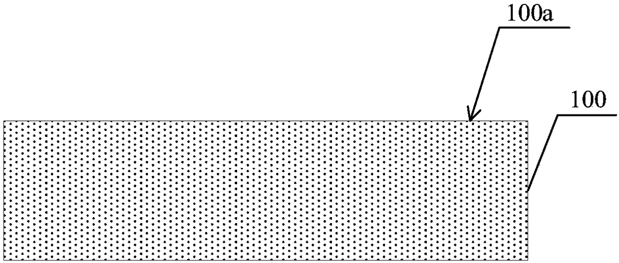
[0049] see Figure 1 to Figure 9(b) . It should be noted that the diagrams provided in this embodiment are only schematically illustrating the basic concept of the present invention, although only the components related to the present invention are shown in the diagrams rather than the number, shape and Dimensional drawing, the shape, quantity and proportion of each component can be changed arbitrarily during actual implementation, an...


PUM


Abstract

The invention provides a thin film heterostructure preparation method. The method comprises steps: a wafer substrate with an injection surface is provided; ion implantation is carried out on the wafersubstrate from the injection surface, and an injection defect layer is formed at a preset depth in the wafer substrate; a support substrate is provided, and the support substrate and the wafer substrate are subjected to temperature rise bonding; the obtained structure is subjected to annealing treatment to form a continuous defect layer; the temperature of the obtained structure is reduced to a preset temperature, reverse thermal stress generated based on temperature reduction strips part of the wafer substrate along the continuous defect layer, and a thin film heterostructure comprising thesupport substrate and the wafer thin film is obtained, wherein the preset temperature is lower than the bonding temperature. In the temperature rise bonding mode, the thermal stress of the bonding structure can be reduced, the bonding structure can keep stable and complete in a high temperature process, the problem of wafer crack generated by thermal mismatch in the stripping process can be effectively solved, and through the reverse thermal stress assisting method, the bonding structure is separated at the continuous defect layer and a bonding interface is not influenced.

Description

technical field [0001] The invention belongs to the technical field of substrate preparation, in particular to a method for preparing a thin film heterostructure. Background technique [0002] With the advent of 5G communications and the development of the Internet of Everything (IOE), the chip technology commonly used in the past can no longer meet people's requirements for high performance, high integration and low power consumption. At this time, people are required to integrate chips with various functions. [0003] According to different material properties, chips based on different materials have their own advantages. For example, silicon chips have the advantages of high integration, gallium arsenide chips have the advantages of high speed and high frequency, gallium nitride chips have the advantages of high power, piezoelectric chips It is widely used in filters of radio frequency systems. To this end, Northrop Grumman Aerospace Sector in the United States integrat...

Claims


Application Information

Patent Timeline
IPC IPC(8): H01L41/312
CPCH10N30/072
Inventor 欧欣黄凯鄢有泉游天桂王曦
Owner 上海新硅聚合半导体有限公司
Why Eureka
Try Eureka