Difunctional device integrating wave plate based on medium meta-surface and optical device

An optical device, a dual-function technology, applied in the direction of optical components, optics, instruments, etc., to achieve the effect of simple structure, easy acquisition and processing, and overcoming the inconvenience of processing and manufacturing

Inactive Publication Date: 2018-09-07
DONGGUAN UNIV OF TECH
View PDF3 Cites 39 Cited by
  • Summary
  • Abstract
  • Description
  • Claims
  • Application Information

AI Technical Summary

Problems solved by technology

According to CN201510974702.4 "a transmissive dual-function device based on gradient metasurface" patent, the multifunctional device needs to combine multiple metasurfaces that can realize their own spec

Method used


Image

  • Difunctional device integrating wave plate based on medium meta-surface and optical device
  • Difunctional device integrating wave plate based on medium meta-surface and optical device
  • Difunctional device integrating wave plate based on medium meta-surface and optical device

Examples


Embodiment 1

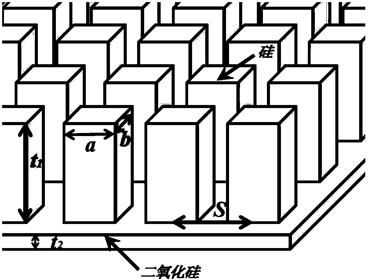
[0020] The specific implementation of the dual-function optical device based on the combination of the wave plate of the dielectric metasurface and the optical device of the present invention is as follows: In this embodiment, the dual-function optical device based on the combination of the wave plate of the dielectric metasurface and the optical device is prepared in the following manner: Silicon is deposited on a molten silicon dioxide substrate by plasma enhanced chemical vapor deposition (PECVD), and then a layer of photoresist is spin-coated on the silicon layer, a selective mask is placed on the photoresist, and ultraviolet light is placed Ultraviolet exposure is carried out in the exposure system, and then the exposed device is put into the developer solution to pattern the photoresist, and then the silicon layer is etched into a brick shape by deep ion etching technology, according to different dual-function devices different size requirements to etch the required silic...

Embodiment 2

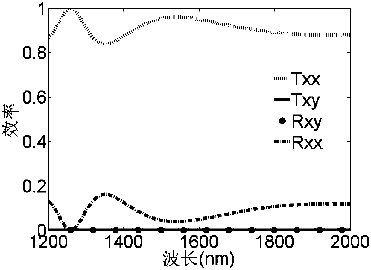
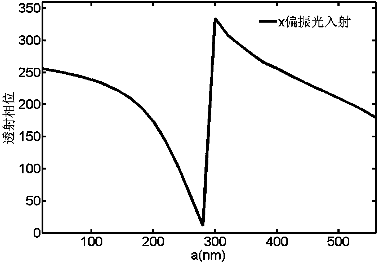
[0032] In this embodiment, a dual-function device that realizes a half-wave plate-deflector and a half-wave plate-focusing lens is used as a specific example to illustrate. The function of one of the wave plates requires two orthogonally polarized light components T to remain transmitted. xx and T yy There is a phase difference of π between them. In addition, it is necessary to ensure that the transmittance of the transmitted orthogonally polarized light is equal. On the basis of realizing the half-wave plate function of polarization conversion, in order to realize the deflector function, this embodiment is the same as the method of embodiment 1, and a period is designed to be 8 metasurface unit structures, and each adjacent two structures The phase difference is π / 4, which satisfies the phase of a period covering 2π; the phases of the eight structural units start from 0 and increase by π / 4 in turn, so as to obtain the phase wavefront required for deflection, and realize the ...


PUM

PropertyMeasurementUnit
Thicknessaaaaaaaaaa
Lattice constantaaaaaaaaaa
Thicknessaaaaaaaaaa

Abstract

The invention discloses a wave plate based on a medium meta-surface, a beam deflector and a difunctional device integrating the wave plate and a focusing lens. The devices work in a communication waveband, silicon is adopted as a dielectric material, and a substrate is made from silicon dioxide. The devices are characterized in that the brick shape of the silicon material serves as the design ofa unit structure, and a plurality of brick-shaped structures conforming to required phase gradient are arranged according to two-dimensional crystal lattice periodicity to form a rectangular array; the thickness of silicon nano-bricks of the unit structures with medium meta-surfaces is 0.9 microns. The transmitted phase difference of an x-line deflection light component and a y-line deflection light component of incident light is controlled by adjusting the length and width of the unit structures while the deflector or the focusing lens is achieved before phase wave control, and accordingly functions of the wave plate are achieved. Compared with existing devices, the devices are simple in structure, and the deflection efficiency is improved to 80%. Compared with existing wave plates and optical devices which are used in a stacked way, processing and manufacturing inconvenience is overcome, and integration and miniaturization of the optical devices are facilitated.

Description

technical field [0001] The invention belongs to the technical field of optical devices based on artificial composite material metasurfaces, in particular to a dual-function device combining a wave plate based on a dielectric metasurface, a beam deflector, a wave plate and a focusing lens. Background technique [0002] Regulating electromagnetic waves has always been a research hotspot in the fields of optics and physics. Traditional optical devices such as analyzers, various lenses, wave plates, and deflectors play a vital role in many fields. However, due to the limitations of the nature of natural materials, as well as the large size and unfavorable integration, many functions cannot be realized. In 2000, an article about negative refraction metamaterials "Negative refraction makes aperfect lens" published in "Physics Review Letter" 85 issue 18 extended the concept of metamaterials. Metamaterials are artificial composite materials composed of subwavelength structural unit...

Claims


Application Information

Patent Timeline
IPC IPC(8): G02B1/00G02B5/30G02B3/00
CPCG02B1/002G02B3/0012G02B3/0037G02B5/3083
Inventor 郭忠义沈飞郭凯周清峰周红平朱烈
Owner DONGGUAN UNIV OF TECH
Why Eureka
Try Eureka