Method for modifying surface of ITO electrode

A technology of electrode surface and indium tin oxide, which is applied in circuits, electrical components, electric solid devices, etc., can solve the problems of uneconomical and high cost, and achieve the effects of saving materials, high power efficiency, and improving current efficiency

Inactive Publication Date: 2018-09-07
WUHAN INSTITUTE OF TECHNOLOGY
View PDF6 Cites 1 Cited by
  • Summary
  • Abstract
  • Description
  • Claims
  • Application Information

AI Technical Summary

Problems solved by technology

In addition, pentacene can also be used as an evaporation protective layer in inverted photoelectric devices to separate the organic functional layer and the top electrode, which is mainly based on the good film stability and compactness of pentacene. As a protective layer, pentacene Benzene

Method used


Image

  • Method for modifying surface of ITO electrode
  • Method for modifying surface of ITO electrode
  • Method for modifying surface of ITO electrode

Examples


Embodiment 1

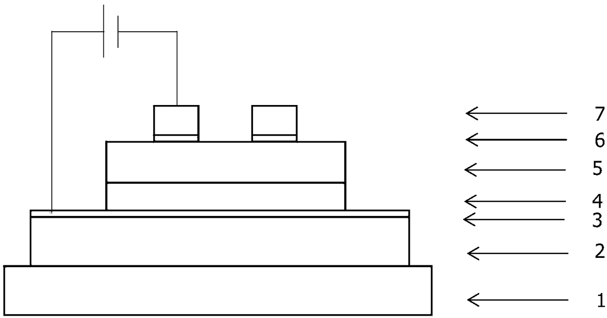
[0033] Embodiment 1: The thickness of the anode interface layer pentacene is selected to be 0.5nm, and the device structure is glass / ITO / pentacene (0.5nm) / NPB (50nm) / Alq 3 (60nm) / LiF(1nm) / Al(150nm).

[0034] When the bottom electrode uses ITO glass as the substrate, the ITO is first photoetched into a strip electrode with a width of 3 mm and a length of 30 mm, and then ultrasonically cleaned with acetone, isopropanol, cleaning agent, and deionized water, and blown with nitrogen. Drying, using a fixed flow of oxygen plasma treatment for 4 minutes; then on the ITO glass substrate, the anode interface layer pentacene (pentacene), the hole transport layer (NPB), the light emitting layer and the electron transport layer (Alq 3 ) cathode interface layer (LiF) and cathode metal (Al), the entire evaporation process is in high vacuum (~10 -4 Pa) environment, and the organic chamber and the metal chamber are operated in the same vacuum environment. Among them, the evaporation rate of ...

Embodiment 2

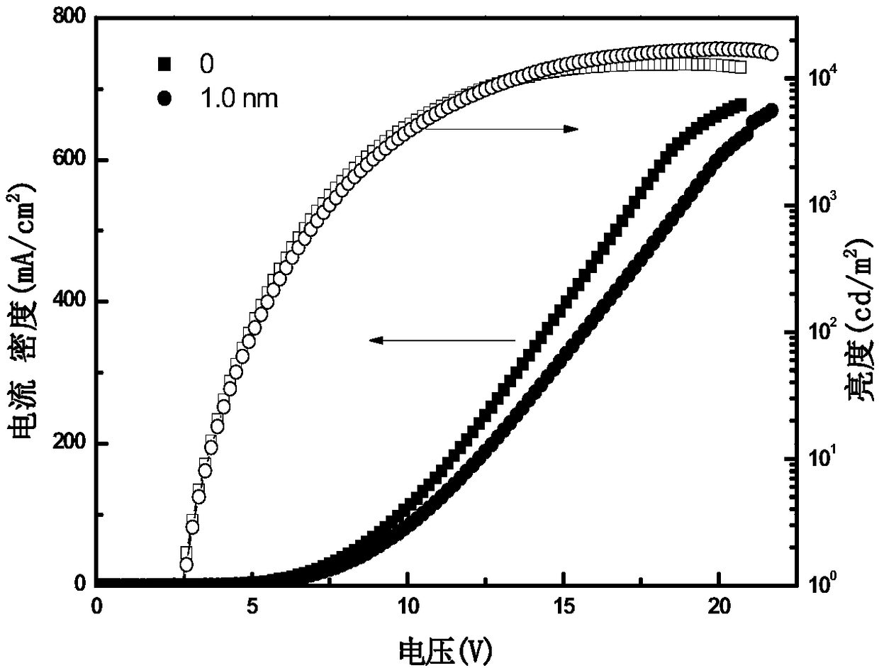
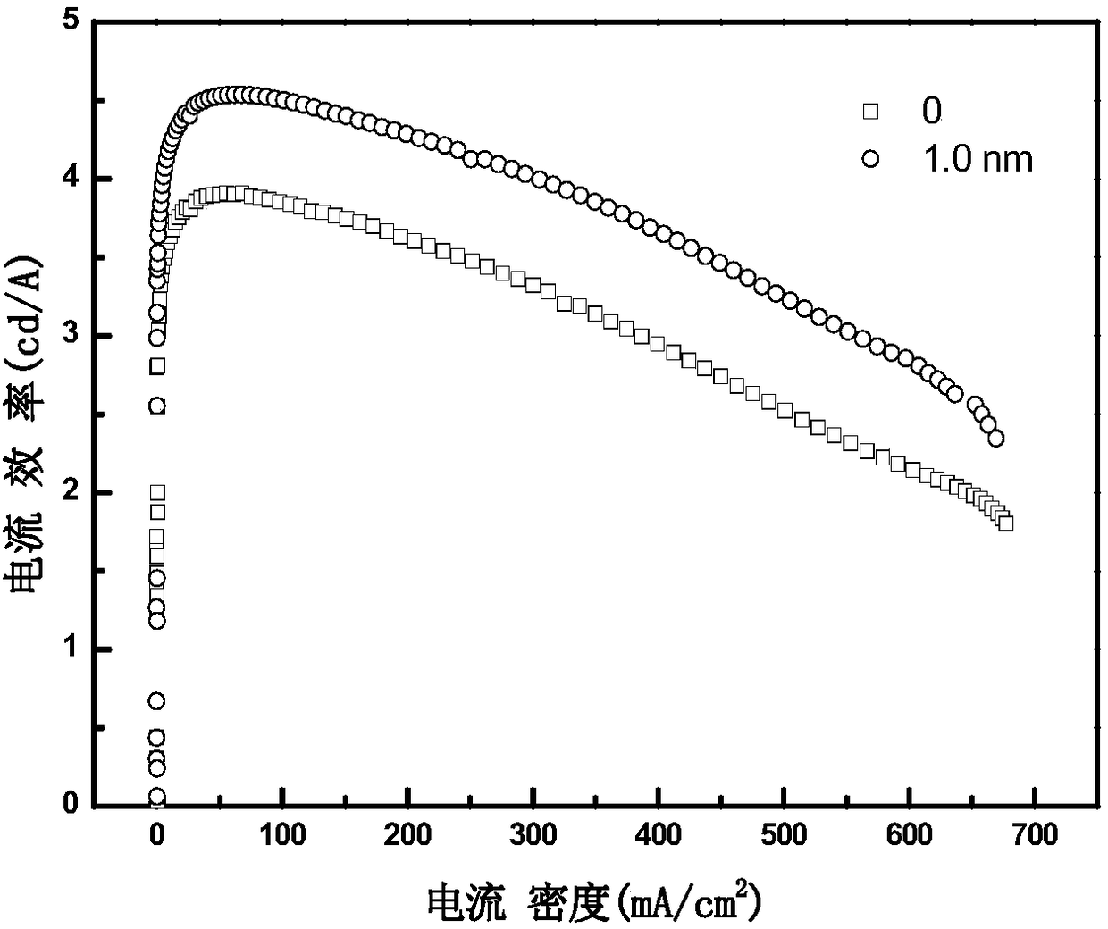
[0035] Example 2: The thickness of the anode interface layer pentacene is selected to be 1.0nm, and the device structure is glass / ITO / pentacene (1.0nm) / NPB (50nm) / Alq 3 (60nm) / LiF(1nm) / Al(150nm).

[0036] When the bottom electrode uses ITO glass as the substrate, the ITO is first photoetched into a strip electrode with a width of 3 mm and a length of 30 mm, and then ultrasonically cleaned with acetone, isopropanol, cleaning agent, and deionized water, and blown with nitrogen. Drying, using a fixed flow of oxygen plasma treatment for 4 minutes; then on the ITO glass substrate, the anode interface layer pentacene (pentacene), the hole transport layer (NPB), the light emitting layer and the electron transport layer (Alq 3 ) cathode interface layer (LiF) and cathode metal (Al), the entire evaporation process is in high vacuum (~10 -4 Pa) environment, and the organic chamber and the metal chamber are operated in the same vacuum environment. Among them, the evaporation rate of pen...

Embodiment 3

[0037] Embodiment 3: The thickness of the anode interface layer pentacene is selected to be 1.5nm, and the device structure is glass / ITO / pentacene (1.5nm) / NPB (50nm) / Alq 3 (60nm) / LiF(1nm) / Al(150nm).

[0038] When the bottom electrode uses ITO glass as the substrate, the ITO is first photoetched into a strip electrode with a width of 3 mm and a length of 30 mm, and then ultrasonically cleaned with acetone, isopropanol, cleaning agent, and deionized water, and blown with nitrogen. Drying, using a fixed flow of oxygen plasma treatment for 4 minutes; then on the ITO glass substrate, the anode interface layer pentacene (pentacene), the hole transport layer (NPB), the light emitting layer and the electron transport layer (Alq 3 ) cathode interface layer (LiF) and cathode metal (Al), the entire evaporation process is in high vacuum (~10 -4 Pa) environment, and the organic chamber and the metal chamber are operated in the same vacuum environment. Among them, the evaporation rate of ...


PUM

PropertyMeasurementUnit
Thicknessaaaaaaaaaa
Thicknessaaaaaaaaaa
Thicknessaaaaaaaaaa

Abstract

The invention relates to a method for modifying a surface of an IOT electrode, which is applied to manufacture of organic photoelectric devices. The method is characterized in that after initial surface cleaning and ultraviolet ozone treatment are performed on an ITO surface, pentacene of which the thickness ranges from 0.5nm to 3.0nm is evaporated to serve as a positive electrode interface layer,then other functional layers of an organic photoelectric device are evaporated, and finally an OLED (Organic Light-Emitting Device) with a structure of ITO/Pentacene/NPB/Alq3/LiF/metal electrode is manufactured, the obtained device is driven by a DC voltage, a driving voltage of the light-emitting device is about 2.9V, the maximum brightness is above 17000cd/m<2>, the maximum current efficiency and the maximum power efficiency respectively reach 4.54cd/A and 2.84lm/w; in comparison with a reference device which is not modified by the pentacene, a lighting voltage is basically unchanged, the maximum brightness increases by more than 30%, the current efficiency increases by 15%, and the power efficiency increases by 27%, at the same time, thin film dimensional stability of an organic functional layer can be improved, and stability of the whole device is also improved.

Description

technical field [0001] The invention relates to the technical field of organic electroluminescent devices, in particular to a method for modifying the surface of an indium tin oxide electrode and an organic electroluminescent diode modified by the method. Background technique [0002] It is generally believed that based on Alq 3 In organic light-emitting diodes (OLEDs), Alq 3 cation formation, while Alq 3 Cations can directly lead to a decrease in the stability and lifetime of the device. In order to solve this problem, many methods have been adopted to control the injection and transport of anode holes, such as doping the hole transport layer, introducing an anode interface layer between the anode and the hole transport layer, and using a mixture of hole and electron transport. emission layer. However, these methods often have great deficiencies. In many cases, due to the reduction of hole injection ability, the operating voltage of the device is significantly increased...

Claims


Application Information

Patent Timeline
IPC IPC(8): H01L51/52H01L51/54H01L51/56
CPCH10K85/623H10K50/81H10K71/00
Inventor 石胜伟李文婷
Owner WUHAN INSTITUTE OF TECHNOLOGY
Why Eureka
Try Eureka