Preparation method of passivation contact type IBC (interdigitated back contact) cell

A battery and equipment technology, applied in the field of solar cells, can solve problems such as laser damage and passivation effect damage, achieve high open circuit voltage and conversion efficiency, reduce silicon wafer damage, and save production costs.

Inactive Publication Date: 2018-09-14
TAIZHOU ZHONGLAI PHOTOELECTRIC TECH CO LTD
View PDF3 Cites 7 Cited by
  • Summary
  • Abstract
  • Description
  • Claims
  • Application Information

AI Technical Summary

Problems solved by technology

If this passivation contact is applied to the back of the IBC, two high-temperature anneals are traditionally required, which will damage the passivation effect; in addition, the interdigitated structure on the back of the traditional IBC battery is generally realized by laser etching, which is easy severe laser damage

Method used


Image

  • Preparation method of passivation contact type IBC (interdigitated back contact) cell
  • Preparation method of passivation contact type IBC (interdigitated back contact) cell
  • Preparation method of passivation contact type IBC (interdigitated back contact) cell

Examples


Embodiment Construction

[0039] The present invention will be described in detail below in conjunction with the embodiments and the accompanying drawings. It should be noted that the described embodiments are only intended to facilitate the understanding of the present invention, rather than limiting it in any way.

[0040] A kind of preparation method of the IBC cell of passivation contact of the present embodiment, comprises the following steps:

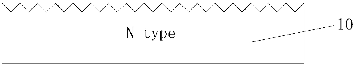
[0041] (1), select the N-type crystalline silicon substrate 10 of 156mm*156mm, and do texture processing to the front surface of the N-type crystalline silicon substrate 10; The resistivity of the N-type crystalline silicon substrate 10 is 0.5~15Ω·cm, preferably 1 ~5Ω·cm; the thickness of the N-type crystalline silicon substrate 10 is 50-300 μm, preferably 80-200 μm; the battery structure after this step is as follows figure 1 shown.

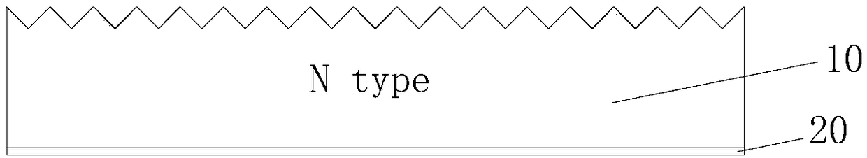
[0042] (2), the back surface oxide layer 20 is grown on the back surface of the N-type crystalline silicon substrate 10, ...


PUM


Abstract

The invention relates to a preparation method of a passivation contact type IBC (interdigitated back contact) cell. A doping processing method for the back surface of an N-type crystalline silicon substrate comprises the following steps: a back surface oxidation layer grows on the back surface of the N-type crystalline silicon substrate, then an intrinsic polycrystalline silicon layer or an intrinsic amorphous silicon layer grows on the back surface oxidation layer, and phosphorus ions are injected into the intrinsic polycrystalline silicon layer or the intrinsic amorphous silicon layer; thena mask grows, an n+ zone is protected by barrier slurry, interdigitated p+ and n+ zones are formed by printing the barrier slurry, the mask in the p+ zone is removed, annealing in the n+ zone and doping in the p+ zone are performed once by boron diffusion finally, and accordingly, alternate p+ and n+ doped zones are formed on the back surface. The preparation method of the passivation contact typeIBC cell has the following beneficial effects: the surface passivation effect is good, and open-circuit voltage and conversion efficiency are high; high-temperature procedures are reduced, and production cost is saved; damage to silicon chips due to laser ablation is reduced, and realization of cells with high conversion efficiency is more facilitated.

Description

technical field [0001] The invention relates to the technical field of solar cells, in particular to a method for preparing a passivated contact IBC cell. Background technique [0002] A solar cell is a semiconductor device that converts light energy into electrical energy. Lower production costs and higher energy conversion efficiency have always been the goals pursued by the solar cell industry. For conventional solar cells, the p+ doped region contact electrodes and the n+ doped region contact electrodes are respectively located on the front and back sides of the battery sheet. The front of the battery is the light-receiving surface, and the coverage of the metal contact electrodes on the front will inevitably cause a part of the incident sunlight to be blocked and reflected by the metal electrodes, resulting in a part of optical loss. The coverage area of ​​the front metal electrode of an ordinary crystalline silicon solar cell is about 7%, and reducing the front covera...

Claims


Application Information

Patent Timeline
Patent Type & Authority Applications(China)
IPC IPC(8): H01L31/18H01L31/0216
CPCH01L31/0216H01L31/18Y02P70/50
Inventor 林建伟何大娟刘志锋张育政
Owner TAIZHOU ZHONGLAI PHOTOELECTRIC TECH CO LTD
Why Eureka
Try Eureka