Passivated contact N-type solar cell, preparation method, assembly and system

A solar cell, N-type technology, applied in the field of solar cells, to achieve good compatibility, high open-circuit voltage and short-circuit current, and reduce the effect of recombination

Inactive Publication Date: 2016-08-24
TAIZHOU ZHONGLAI PHOTOELECTRIC TECH CO LTD
View PDF6 Cites 23 Cited by
  • Summary
  • Abstract
  • Description
  • Claims
  • Application Information

AI Technical Summary

Problems solved by technology

Using point contact electrodes or similar methods can only alleviate the problem to some extent but not eradicate it

Method used


Image

  • Passivated contact N-type solar cell, preparation method, assembly and system
  • Passivated contact N-type solar cell, preparation method, assembly and system
  • Passivated contact N-type solar cell, preparation method, assembly and system

Examples


Embodiment 1

[0033] see Figure 1 to Figure 6 As shown, a method for preparing a passivated contact N-type solar cell of the present embodiment mainly includes the following steps:

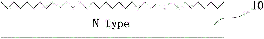
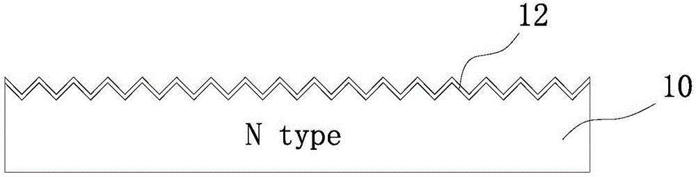
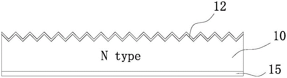
[0034] (1), select the N-type crystalline silicon substrate 10 of 156mm * 156mm, and do texture processing to the front surface of the N-type crystalline silicon substrate 10; The resistivity of the N-type crystalline silicon substrate 10 is 0.5~15Ω·cm, preferably 1 ~5Ω·cm; the thickness of the N-type crystalline silicon substrate 10 is 50-300 μm, preferably 80-200 μm; the battery structure after this step is as follows figure 1shown.

[0035] (2), put the N-type crystalline silicon substrate 10 processed in step (1) into an industrial diffusion furnace to carry out boron diffusion to the suede surface to form a front p+ doped region 12, the boron source adopts boron tribromide, and the diffusion The temperature is 900-1000° C., and the time is 60-180 minutes. The square resistance after boron diffusion is ...

Embodiment 2

[0044] (1), select the N-type crystalline silicon substrate 10 of 156mm * 156mm, and do texture processing to the front surface of the N-type crystalline silicon substrate 10; The resistivity of the N-type crystalline silicon substrate 10 is 0.5~15Ω·cm, preferably 1 ~5Ω·cm; the thickness of the N-type crystalline silicon substrate 10 is 50-300 μm, preferably 80-200 μm; the battery structure after this step is as follows figure 1 shown.

[0045] (2), put the N-type crystalline silicon substrate 10 processed in step (1) into an industrial diffusion furnace to carry out boron diffusion to the suede surface to form a front p+ doped region 12, the boron source adopts boron tribromide, and the diffusion The temperature is 900-1000° C., and the time is 60-180 minutes. The square resistance after boron diffusion is 40-100Ω / sqr, preferably 50-70Ω / sqr.

[0046] (3) Put the boron-diffused N-type crystalline silicon substrate 10 into an etching cleaning machine, and remove the boron dif...


PUM

PropertyMeasurementUnit
electrical resistivityaaaaaaaaaa
thicknessaaaaaaaaaa
thicknessaaaaaaaaaa

Abstract

The invention relates to a passivated contact N-type solar cell, a preparation method, an assembly and a system. The preparation method for a passivated contact N-type solar cell includes the steps of conducting doping treatment for the front surface of an N-type crystalline silicon substrate to form a p+ doped region; preparing a tunneling oxide layer on the back surface of the N-type crystalline silicon substrate, then preparing a phosphorus-containing amorphous silicon layer or phosphorus-containing polysilicon layer on the tunneling oxide layer, and then conducting annealing; and after preparation of passivated anti-reflection film and a passivated film, printing and sintering metal slurry to obtain a front electrode and a back electrode. The beneficial effects of the invention lie in that the tunneling oxide layer can provide the silicon substrate with an excellent surface passivated effect and achieve selective tunneling of carriers, the n+ doped polysilicon layer can effectively transmit the carriers for the metal electrode on the back surface to collect, the back metal electrode does not destroy the passivated layer on the surface of the crystalline silicon substrate, and thus thereby open-circuit voltage of the cell can be greatly increased.

Description

technical field [0001] The invention relates to the technical field of solar cells, in particular to a passivated contact N-type solar cell, a preparation method, an assembly, and a system. Background technique [0002] A solar cell is a semiconductor device that converts solar energy into electrical energy, and its key indicator is photoelectric conversion efficiency. A variety of factors will affect the photoelectric conversion efficiency, among which the passivation quality of the silicon substrate surface is a more critical factor. The quality of passivation is good, and the surface recombination rate of the silicon substrate is low, so that higher open circuit voltage and short circuit current can be obtained, so the surface passivation of solar cells has always been the top priority of design and optimization. The common passivation method in the industry is to grow a passivation film on the surface of the silicon substrate. The common passivation film is SiO 2 、SiN ...

Claims


Application Information

Patent Timeline
Patent Type & Authority Applications(China)
IPC IPC(8): H01L31/18H01L31/0236
CPCH01L31/02366Y02E10/50Y02P70/50
Inventor 林建伟孙玉海刘志锋季根华张育政
Owner TAIZHOU ZHONGLAI PHOTOELECTRIC TECH CO LTD
Why Eureka
Try Eureka