Eureka AIR delivers breakthrough ideas for toughest innovation challenges, trusted by R&D personnel around the world.

N-type organic semiconductor material as well as perpetration method and application thereof

An organic semiconductor, n-type technology, applied in the field of n-type organic semiconductor materials and its preparation, can solve the problems of limiting carrier mobility and absorption coefficient, and difficult to optimize photoelectric performance

Active Publication Date: 2018-09-21
SOUTH UNIVERSITY OF SCIENCE AND TECHNOLOGY OF CHINA
View PDF3 Cites 2 Cited by
  • Summary
  • Abstract
  • Description
  • Claims
  • Application Information

AI Technical Summary

Problems solved by technology

Despite the excellent device performance, the twisted framework of NDIs and PDIs based polymers limits their carrier mobility and absorption coefficient. In addition, the challenges in synthesis and the steric hindrance effect of the bay site make the NDIs and PDIs framework Functionalization is extremely challenging, so their optoelectronic properties are difficult to optimize

Method used


Image

  • N-type organic semiconductor material as well as perpetration method and application thereof
  • N-type organic semiconductor material as well as perpetration method and application thereof
  • N-type organic semiconductor material as well as perpetration method and application thereof

Examples


Embodiment 1

[0217] This embodiment prepares the brominated monomer (compound 10) of the n-type organic semiconductor material having the structure shown in formula II through the following steps:

[0218] Step (1): Synthesis of Compound 2

[0219]

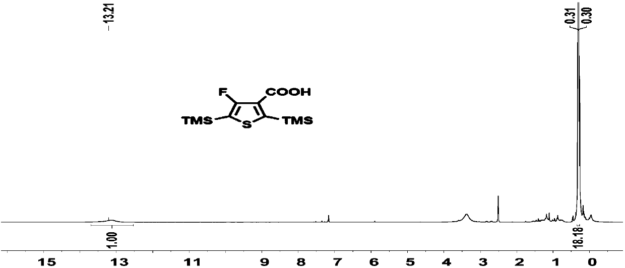
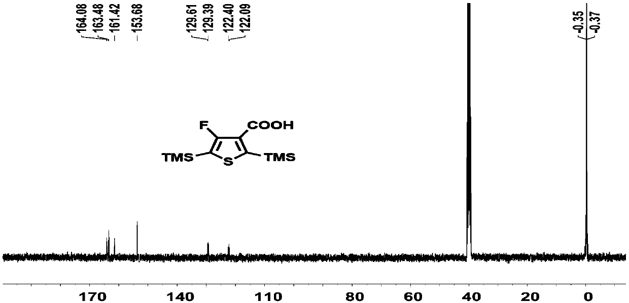
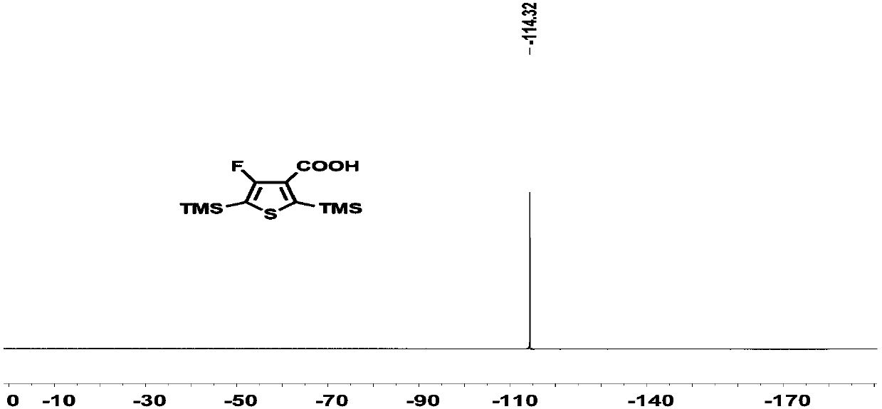
[0220] Compound 1 (4.1 g, 12.6 mmoL) was dissolved in 100 mL of ether solution. Add n-butyllithium (2.4M, 7.8mL, 1.05eq) at -78°C to react for 1 hour, and then pass excess carbon dioxide gas. Reaction 1h rose to room temperature. The solvent was removed under reduced pressure, the remaining solid was dissolved in water, concentrated hydrochloric acid was added dropwise on an ice-water bath until a white solid precipitated, filtered and washed with water until neutral, and dried in a vacuum oven to obtain compound 2 (3.1 g, yield: 96%), directly for the next step. H NMR spectrum such as Figure 1A As shown, the carbon NMR spectrum is as Figure 1B As shown, the NMR fluorine spectrum is shown as Figure 1C As shown, high-resolution mass ...

Embodiment 2

[0255] In this embodiment, an n-type organic semiconductor material having a structure shown in formula II is prepared through the following steps:

[0256]

[0257] Add the tinned monomer (37.34, 0.083mmoL, 1.0eq) and the brominated monomer compound 4 (0.102g, 0.083mmoL) into a 5mL reaction tube, and at the same time add the catalyst Pd 2 (dba) 3 (1.09mg, 0.0012mmol, 1.5%eq), Ligand P(o-tolyl)3 (3.03 mg, 0.010 mmol, 12% eq) with argon sparging. Finally, 2.5 mL of anhydrous toluene was added. The reaction tube was placed in a microwave reactor and reacted at 140°C for 3 hours. After cooling to room temperature, 2-tributyltinthiophene was added, and capped at 100°C for 20 minutes. After cooling down to room temperature again, the reaction liquid was added into methanol, stirred for 3 hours, precipitated, filtered, and further extracted with methanol through a fat extractor to take out low molecular weight products. Finally, the product was concentrated, dropped into 5 mL...

Embodiment 3

[0261] UV absorption spectrum, electrochemical test and thermal stability characterization

[0262] UV-Vis absorption spectra and cyclic voltammetry of polymer s-FBTI2-FT in solution and film states Figure 10 and 11 As shown, the introduction of F atoms does not affect the energy level (E g opt =1.96eV), effectively lowering the molecular orbital energy level of the polymer molecule (HOMO=-5.54eV; LUMO=-3.57eV). It is more conducive to the injection and transmission of carriers in transistors, and has better energy level matching and spectral complementarity with polymer donors in all-polymer solar cells, which is conducive to the absorption of photons and the increase of current. In addition, polymers have good thermal stability, such as Figure 12 As shown, the mass loss of the polymer is 5% at over 400°C.


PUM


Abstract

The invention provides an n-type organic semiconductor material as well as a perpetration method and application thereof. The n-type organic semiconductor material has a structure shown as a formula Ior a formula VII. The n-type organic semiconductor material prepared by the preparation method provided by the invention has high electronic transmission performance, excellent solubility, high skeleton planarity, good crystallinity and controllable photoelectric property, not only can be taken as a receptor material for an all-polymer solar cell, but also can be taken as an electronic transmission material in a n-type field effect transistor and has huge application potentials and values in the field of organic semiconductor materials.

Description

technical field [0001] The invention belongs to the field of semiconductors, and relates to an n-type organic semiconductor material and its preparation method and application. Background technique [0002] At present, low-cost, large-area, and solution-processable electronic devices based on polymer semiconductors have attracted great attention both in the field of basic scientific research and in the industrial field of practical applications. Especially in the field of organic thin film transistors (OTFTs) and polymer solar cells (PSCs), a large number of hole transport materials have been used in field effect transistor devices in recent years, and their performance has been improved to a level comparable to that of inorganic materials. In solar energy, p-type materials are widely used in the study of donor materials. However, due to the challenges of chemical synthesis and achieving low frontier molecular orbital energy levels, the variety and device performance of n-t...

Claims


Application Information

Patent Timeline
Patent Type & Authority Applications(China)
IPC IPC(8): C08G61/12
CPCC08G61/121C08G61/126C08G2261/124C08G2261/1412C08G2261/1646C08G2261/18C08G2261/3229C08G2261/414C08G2261/51
Inventor 郭旭岗孙会靓汤育民郭晗
Owner SOUTH UNIVERSITY OF SCIENCE AND TECHNOLOGY OF CHINA
Why Eureka
Eureka Blog
Learn More