Cadmium zinc telluride radiation sensitive field effect transistor and preparation method thereof

A field effect transistor and radiation-sensitive technology are applied in the field of cadmium zinc telluride nuclear radiation detectors and their preparation, which can solve the problems of unsatisfactory performances such as high-energy ray capture ability and sensitivity of the cadmium zinc telluride detector, and achieve easy growth, good performance

Inactive Publication Date: 2020-01-17
SHANGHAI UNIV
View PDF7 Cites 0 Cited by
  • Summary
  • Abstract
  • Description
  • Claims
  • Application Information

AI Technical Summary

Problems solved by technology

[0006] Due to the high resistance of CdZnTe crystals and the fact that most of them are P-type semiconductors, most of the research on CdZnTe nuclear radiation detectors is devoted to the design of electrode structures, such as Frisch grid detectors and coplanar grid detectors. The CdZnTe detector for the device structure is rarely studied, and the high-energy ray capture ability and sensitivity of the CdZnTe detector are not ideal enough, which has become a technical problem that needs to be solved urgently

Method used


Image

  • Cadmium zinc telluride radiation sensitive field effect transistor and preparation method thereof
  • Cadmium zinc telluride radiation sensitive field effect transistor and preparation method thereof
  • Cadmium zinc telluride radiation sensitive field effect transistor and preparation method thereof

Examples


Embodiment 1

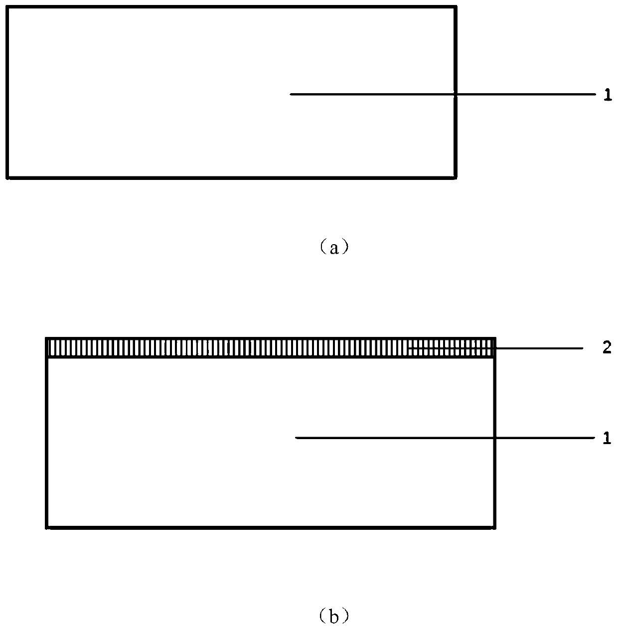
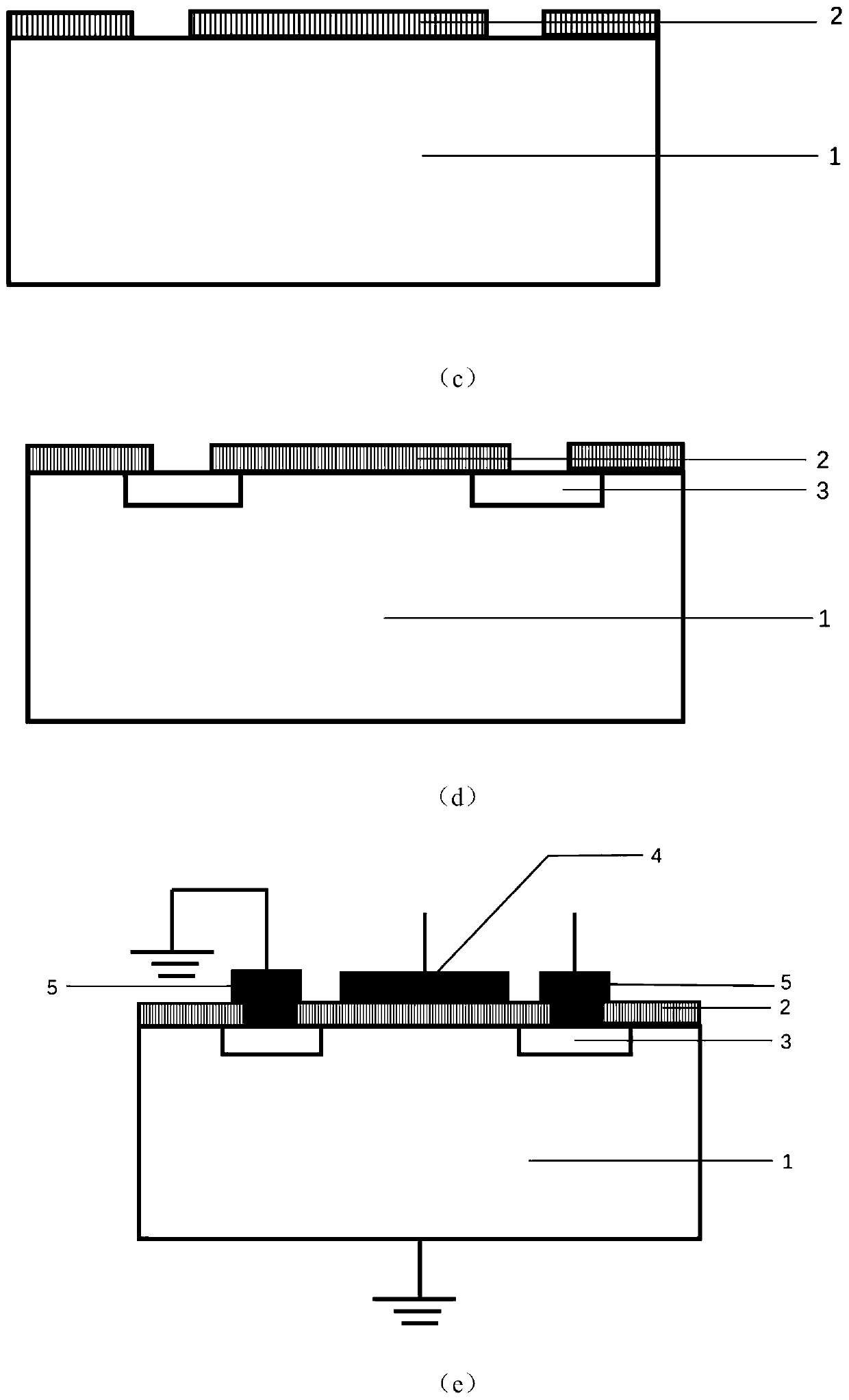
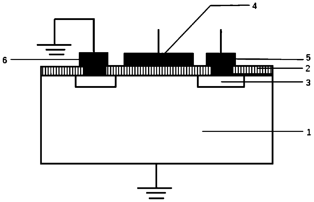
[0031] In this example, see figure 1 and figure 2 , a cadmium zinc telluride radiation-sensitive field effect transistor, comprising a substrate 1, a gate electrode 4, a gate insulating layer 2, a channel layer 3 and a source-drain electrode 5; a gate insulating layer 2 is formed on the substrate 1, and the gate insulating layer The gate electrode 4 is formed on the layer 2, the channel layer 3 is embedded in the surface layer of the substrate 1, and the source electrode and the drain electrode are respectively formed on the surfaces of the two adjacent channel layers 3 to form the source-drain electrode 5 functional layer. The electrode 5 passes through the patterned hole of the gate insulating layer 2, the gate electrode 4 is formed on the surface of the gate insulating layer 2 between two adjacent channel layers 3, and the materials of the substrate 1 and the gate insulating layer 2 are all made of It is made of CdZnTe material, wherein the substrate 1 is made of low-resi...

Embodiment 2

[0041] This embodiment is basically the same as Embodiment 1, especially in that:

[0042] In this embodiment, the channel layer 3 is formed by doping indium ions into the low-resistance CdZnTe material of the substrate 1 . The resistivity of the low-resistance CdZnTe crystal material used in substrate 1 is 10 7 Ω·cm, the conductivity type is P-type. The resistivity of the high-resistance CdZnTe thin film used as the gate insulating layer 2 is 10 11 Ω·cm, the conductivity type is N type. Au / Cr composite electrodes are used for the gate electrode 4 and the source-drain electrode 5 . The thickness of the substrate 1 is 2 mm, the thickness of the high-resistance cadmium zinc telluride film as the gate insulating layer 2 is 400 μm, and the thickness of the channel layer is 80 μm; the aspect ratio of the overall device of the zinc cadmium radiation sensitive field effect transistor is 30 / 6mm .

[0043] In this embodiment, a method for preparing a cadmium zinc telluride radiati...

Embodiment 3

[0051] This embodiment is basically the same as the previous embodiment, and the special features are:

[0052] In this embodiment, the channel layer 3 is formed by doping indium ions into the low-resistance CdZnTe material of the substrate 1 . The resistivity of the low-resistance CdZnTe crystal material used in substrate 1 is 10 5 Ω·cm, the conductivity type is P-type. The resistivity of the high-resistance CdZnTe thin film used as the gate insulating layer 2 is 10 9 Ω·cm, the conductivity type is N type. Au / Cr composite electrodes are used for the gate electrode 4 and the source-drain electrode 5 . The thickness of the substrate 1 is 2 mm, the thickness of the high-resistance cadmium zinc telluride film as the gate insulating layer 2 is 400 μm, and the thickness of the channel layer is 80 μm; the aspect ratio of the overall device of the zinc cadmium radiation sensitive field effect transistor is 30 / 6mm .

[0053] In this embodiment, a method for preparing a cadmium zi...


PUM

PropertyMeasurementUnit
electrical resistivityaaaaaaaaaa
thicknessaaaaaaaaaa

Abstract

The invention discloses a cadmium zinc telluride radiation sensitive field effect transistor and a preparation method thereof. A radiation sensitive field effect transistor is formed on a cadmium zinctelluride substrate; a gate insulating layer of the device is a high-resistance cadmium zinc telluride thin film, so that the capturing capability and sensitivity of the detector on high-energy rayscan be reinforced; the low-resistance cadmium zinc telluride substrate is used as a channel layer and matched with the lattice constant of the insulting layer, so that device stability is improved; byperforming an ion injection process on the low-resistance cadmium zinc telluride substrate, and by introducing high-concentration impurity traps, the threshold voltage of the device can be adjusted effectively, source drain contact resistance can be lowered, and device sensitivity is improved; and the RadFET structural detector has a simple process and relatively low requirement on cadmium zinc telluride crystals, is suitable for detection of radiation dosage and has wide application prospect.

Description

technical field [0001] The invention relates to a semiconductor nuclear radiation detector and a preparation method thereof, in particular to a cadmium zinc telluride nuclear radiation detector and a preparation method thereof, which are applied in semiconductor device manufacturing, nuclear physics, X-ray and gamma-ray astronomy and field of nuclear medicine technology. Background technique [0002] In recent years, the development of semiconductor nuclear radiation detectors is quite rapid. Such detectors have been widely used in many fields such as nuclear physics, X-ray and gamma-ray astronomy, and nuclear medicine. Compared with gas detectors and scintillator detectors, semiconductor detectors have better imaging performance and stronger spectral resolution capabilities, and can also make the structure of the entire detection system more compact. Among semiconductor detectors, CdZnTe detectors are one of the most competitive detectors. CdZnTe crystals have a large ba...

Claims


Application Information

Patent Timeline
Patent Type & Authority Patents(China)
IPC IPC(8): H01L31/119H01L31/032H01L31/18
CPCH01L31/032H01L31/119H01L31/18Y02P70/50
Inventor 王处泽张继军闵嘉华薛瑶王林军梁小燕师好智黄健唐可凌立文
Owner SHANGHAI UNIV
Why Eureka
Try Eureka