Infrared transparent window with electromagnetic shielding function and preparation method of infrared transparent window

A technology for electromagnetic shielding and transparent windows, which is applied in the field of infrared transparent windows and its preparation, can solve problems such as the difficulty of achieving high infrared transmittance and high electromagnetic shielding efficiency at the same time, so as to improve electromagnetic shielding efficiency, improve the ability to resist electromagnetic interference, The effect of improving crystal quality

Active Publication Date: 2018-11-02
SUN YAT SEN UNIV
View PDF6 Cites 6 Cited by
  • Summary
  • Abstract
  • Description
  • Claims
  • Application Information

AI Technical Summary

Problems solved by technology

Tin-doped indium oxide (ITO) is a commonly used transparent conductive material, but in general the mobility is only 10-40cm 2 / Vs, it is difficult to achieve high infrared transmittance and high electromagnetic shielding efficiency at the same time

Method used


Image

  • Infrared transparent window with electromagnetic shielding function and preparation method of infrared transparent window
  • Infrared transparent window with electromagnetic shielding function and preparation method of infrared transparent window
  • Infrared transparent window with electromagnetic shielding function and preparation method of infrared transparent window

Examples


Embodiment 1

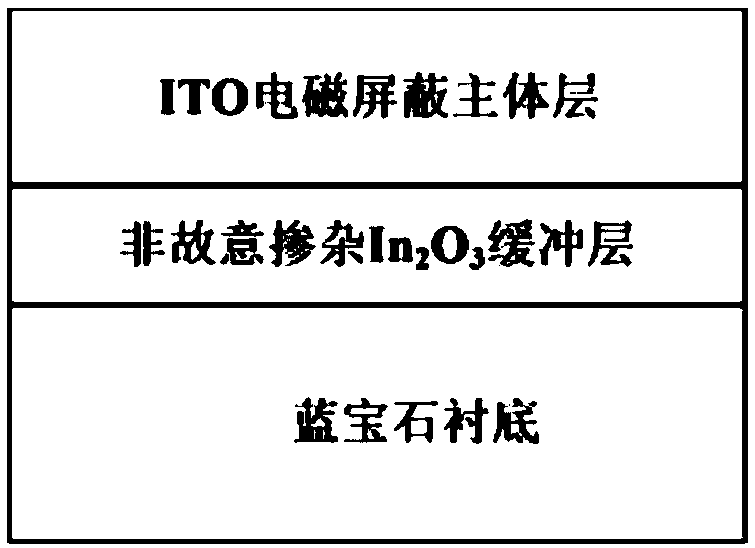
[0040] An infrared window containing a high mobility electromagnetic shielding layer.

[0041] Step 1: Select a clean sapphire substrate with a 0.2° deviation angle between the surface and the c crystal plane, double-sided polishing, and a thickness of 430 μm.

[0042] Step 2: Send the substrate into the reaction chamber of the MOCVD equipment, and let the tray rotate at a speed of 750 rpm;

[0043] Step 3: The temperature of the reaction chamber is raised to 630° C.; at the same time, 10 slm of argon gas is introduced into the reaction chamber, and the pressure of the reaction chamber is controlled at 9 Torr through the pressure control system.

[0044] Step 4: Immerse the bubbling bottle containing trimethylindium and tetrakis(dimethylamino)tin in two constant temperature water tanks, control the temperature of the bubbling bottle to 25°C and 5°C through the constant temperature water tank, and pass the mass flow meter And pressure gauge, control the pressure of two bubblin...

Embodiment 2

[0054] An infrared window comprising an electromagnetic shielding main body layer with non-uniform distribution of doping concentration.

[0055] Step 1: Select a clean sapphire substrate with a 0.2° deviation angle between the surface and the c crystal plane, double-sided polishing, and a thickness of 430 μm.

[0056] Step 2: Send the substrate into the reaction chamber of the MOCVD equipment, and let the tray rotate at a speed of 750 rpm;

[0057] Step 3: The temperature of the reaction chamber is raised to 630° C.; at the same time, 10 slm of argon gas is introduced into the reaction chamber, and the pressure of the reaction chamber is controlled at 9 Torr through the pressure control system.

[0058] Step 4: Immerse the bubbling bottle containing trimethylindium and tetrakis(dimethylamino)tin in two constant temperature water tanks, control the temperature of the bubbling bottle to 25°C and 5°C through the constant temperature water tank, and pass the mass flow meter And ...

Embodiment 3

[0067] An infrared window containing a high mobility electromagnetic shielding layer.

[0068] Step 1: Select a clean sapphire substrate with a 2° deviation angle between the surface and the c crystal plane, a thickness of 100 μm, and double-sided polishing.

[0069] Step 2: Send the substrate into the reaction chamber of the MOCVD equipment, and let the tray rotate at a speed of 750 rpm;

[0070] Step 3: The temperature of the reaction chamber is raised to 900° C.; at the same time, 10 slm of argon gas is introduced into the reaction chamber, and the pressure of the reaction chamber is controlled at 760 Torr through the pressure control system.

[0071] Step 4: Immerse the bubbling bottle containing trimethylindium and tetrakis(dimethylamino)tin in two constant temperature water tanks, control the temperature of the bubbling bottle to 25°C and 5°C through the constant temperature water tank, and pass the mass flow meter And pressure gauge, control the pressure of two bubblin...


PUM

PropertyMeasurementUnit
thicknessaaaaaaaaaa
thicknessaaaaaaaaaa
thicknessaaaaaaaaaa

Abstract

The invention discloses an infrared transparent window with an electromagnetic shielding function. The infrared transparent window is prepared from a sapphire substrate and an ITO (indium oxide) basedsemiconductor film lamination located above the sapphire substrate with a metal organic chemical vapor deposition method, wherein a deviation angle of 0-2 degrees is formed between the surface of thesapphire substrate and the c crystal face of sapphire, and the sapphire substrate is subjected to double-sided polishing, and the thickness of the sapphire substrate is 100-10000 mu m; the ITO basedsemiconductor film lamination is prepared from an unintentionally doped ITO buffer layer and an Sn-doped ITO electromagnetic shielding main body layer by laminating; the thickness of the unintentionally doped ITO buffer layer is 10-1000 nm, and electron mean concentration is not higher than 1*10<19>cm<-3>; the thickness of the electromagnetic shielding main body layer is 0.2-200 mu m, and electronmean concentration is not higher than 5*10<19>cm<-3>. Square resistance of the infrared transparent window is lower than 100 omega / sq, the transmittance of the infrared transparent window in a wavelength range of 0.78-2.5 mu m is higher than 70%, the transmittance of the infrared transparent window in a wavelength range of 2.5-5 mu m is higher than 50%, electron mobility is higher than 70 cm<2> / Vs, and electromagnetic shielding efficiency in a frequency range of 1-18 GHz is higher than 12 dB.

Description

technical field [0001] The invention belongs to the field of infrared optical materials and thin film materials, and mainly relates to an infrared transparent window with electromagnetic shielding function and a preparation method thereof. Background technique [0002] Due to the obvious thermal effect of infrared rays, infrared technology has received extensive attention in both military and civilian fields. Specific bands of infrared (such as 3-5 μm mid-infrared) have strong penetrating ability in the atmospheric environment, so infrared detection is suitable for long-distance (such as air-to-ground) detection and positioning. However, when using infrared technology to detect long-distance targets, the target signal strength is weak, so infrared detection technology is extremely susceptible to electromagnetic wave interference in the atmospheric environment. This actual situation puts forward higher requirements for the electromagnetic shielding ability of the infrared de...

Claims


Application Information

Patent Timeline
Patent Type & Authority Applications(China)
IPC IPC(8): C23C16/40C23C16/02H01B5/14H01B13/00H05K9/00
Inventor 陈梓敏王钢卓毅
Owner SUN YAT SEN UNIV
Why Eureka
Try Eureka