A method for manufacturing a Gan-based LED-encapsulated electrode structure

A technology of electrode structure and manufacturing method, which is applied to circuits, electrical components, semiconductor devices, etc., can solve the problems of difficulty in completing side reflections, and the edges of electrodes cannot be effectively and completely covered, and achieve the effect of improving brightness.

Active Publication Date: 2019-10-25
SHANDONG INSPUR HUAGUANG OPTOELECTRONICS
View PDF8 Cites 0 Cited by
  • Summary
  • Abstract
  • Description
  • Claims
  • Application Information

AI Technical Summary

Problems solved by technology

However, this patent does not involve a specific method of manufacturing coated electrodes. In the manufacture of traditional electrodes, most of them are stacked structures, which cannot be effectively and completely covered at the edge of the electrode, and side reflection is difficult to complete.

Method used


Image

  • A method for manufacturing a Gan-based LED-encapsulated electrode structure
  • A method for manufacturing a Gan-based LED-encapsulated electrode structure
  • A method for manufacturing a Gan-based LED-encapsulated electrode structure

Examples


Embodiment 1

[0056] A method for manufacturing a GaN-based LED coated electrode structure, comprising the following steps:

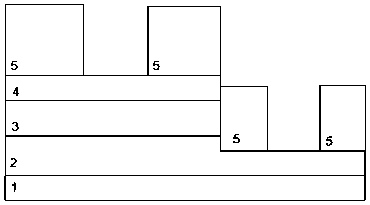
[0057] Step 1, the first photolithography electrode pattern production, on the GaN-based LED wafer, use negative photoresist to make photolithography electrode pattern; figure 1 shown;

[0058] Step 2, the first evaporation electrode, including:

[0059] Step 2-1, place the wafer completed in step 1 in the chamber of the electron beam evaporation table, and after the vacuum degree reaches 9.0E-6 Torr, evaporate the first Cr layer with a thickness of 5 angstroms, and cool for 3 minutes;

[0060] Step 2-2, performing evaporation of the first Al layer reflector with a thickness of 500 angstroms, and cooling for 3 minutes;

[0061] Step 2-3, performing Ti layer vapor deposition with a thickness of 200 angstroms, and cooling for 3 minutes;

[0062] Step 2-4, conduct Au layer evaporation with a thickness of 3000 angstroms, and cool to room temperature 25°;

[0063] Ste...

Embodiment 2

[0074] A method for manufacturing a GaN-based LED coated electrode structure, comprising the following steps:

[0075] Step 1. The first photolithographic electrode pattern production, using negative photoresist on the GaN-based LED wafer, to produce photolithographic electrode patterns;

[0076] Step 2, the first evaporation electrode, including:

[0077] Step 2-1, place the wafer completed in step 1 in the chamber of the electron beam evaporation table, and after the vacuum degree reaches 9.0E-6 Torr, evaporate the first Cr layer with a thickness of 30 angstroms, and cool for 3 minutes;

[0078] Step 2-2, performing evaporation of the first Al layer reflector with a thickness of 1000 angstroms, and cooling for 3 minutes;

[0079] Step 2-3, performing Ti layer vapor deposition with a thickness of 500 angstroms, and cooling for 3 minutes;

[0080] Step 2-4, conduct Au layer evaporation, the thickness is 5000 Angstrom, cool to room temperature 25 °;

[0081] Step 2-5, use th...

Embodiment 3

[0090] A method for manufacturing a GaN-based LED coated electrode structure, the steps of which are as described in Example 1, except that in steps 2-5, the mass fraction of hydrochloric acid is 36%, and the density of the hydrochloric acid is 1.10 g / ml.


PUM


Abstract

The invention relates to a method for manufacturing a GaN-based LED coated electrode structure, which belongs to the technical field of semiconductor processing, and comprises the following specific steps: 1. Making photolithographic electrode patterns for the first time; 2. Evaporating Cr and Al on electrodes for the first time , Ti, Au; 3. The second photolithographic electrode pattern production; 4. Oxygen plasma cleaning; 5. The second electrode evaporation. The present invention realizes the manufacture of the coated electrode structure through two times of photolithographic electrode pattern and two times of electrode evaporation. Through the double-sided reflection of the electrode, the luminous brightness of the entire tube core is extremely high; through the cleaning of oxygen plasma, it is guaranteed overall electrode stability. The principle of the whole production process is simple. The tube core produced by the method of the present invention has high luminous brightness, high yield rate of the tube core bonding wire, and good overall stability of the electrode. This method is applicable to the production of all GaN-based LED tube cores, suitable for wide range.

Description

technical field [0001] The invention relates to a specific manufacturing method of a GaN-based LED coated electrode structure with double-sided reflection function, and belongs to the technical field of semiconductor processing. Background technique [0002] LED (Light Emitting Diode), a light-emitting diode, is a solid-state semiconductor light-emitting device that can directly convert electrical energy into light energy. The key structure of the LED is a semiconductor wafer, one end of the wafer is attached to a bracket and used as the negative pole (N pole), and the other end is connected to the positive pole (P pole) of the power supply, and the entire wafer is sealed by epoxy resin . The semiconductor wafer consists of two parts (P, N electrodes), one part is a P-type semiconductor, in which holes dominate the P-type semiconductor, the other end is an N-type semiconductor, and the N-type semiconductor is mainly electrons, usually in the middle. Quantum wells of 1 to 5...

Claims


Application Information

Patent Timeline
Patent Type & Authority Patents(China)
IPC IPC(8): H01L33/36H01L33/38H01L33/32H01L33/00
CPCH01L33/0075H01L33/32H01L33/36H01L33/38
Inventor 徐晓强刘琦闫宝华彭璐郑兆河徐现刚
Owner SHANDONG INSPUR HUAGUANG OPTOELECTRONICS
Why Eureka
Try Eureka