Silicon carbide epitaxial wafer, silicon carbide insulated gate bipolar transistor, and method of manufacturing the same
A technology of bipolar transistors and epitaxial wafers, which is applied in semiconductor/solid-state device manufacturing, semiconductor devices, electrical components, etc., can solve problems such as increased production efficiency costs, increased resistance of epitaxial wafers, and decreased yields, and achieves suppression The effect of stacking faults
- Summary
- Abstract
- Description
- Claims
- Application Information
AI Technical Summary
Problems solved by technology
Method used
Image


Examples
no. 1 approach -
[0031]
[0032] refer to figure 1 A silicon carbide insulated gate bipolar transistor (hereinafter also referred to as "first SiC-IGBT") according to the first embodiment will be described. The first SiC-IGBT has a p-type buffer layer 2 doped with Al and B, an n-type field stop layer 3 disposed on the p-type buffer layer 2, and an n-type field stop layer disposed on the n-type field stop layer 3. - Type pressure sustaining layer 4.
[0033] In the n-type field stop layer 3, for example with ratio n - Nitrogen (N) is added to the impurity concentration (hereinafter also simply referred to as "concentration") of the type breakdown voltage sustaining layer 4 at a high concentration. in n - type withstand voltage sustaining layer 4, for example with about 1×10 15 cm -3 N is added below. Determine n appropriately according to the specified withstand voltage - The thickness of the type withstand voltage maintaining layer 4. For example, if the withstand voltage of the fir...
Embodiment 1
[0075] Next, Example 1 using the first SiC-IGBT manufacturing method will be specifically described. First, for an n that is biased by 4° in the direction + The Si surface of the substrate formed by type 4H-SiC is subjected to CMP, and the diameter 350µm thick n- + Type Substrate 1. Then, the produced n + The substrate 1 is transported to the epitaxial growth device.
[0076] Then, in an environment with a temperature of about 1640°C and a pressure of about 4kPa, as a raw material gas, the 3 / s (40slm) flow into hydrogen (H 2 ), with about 0.1014Pa·m 3 / s (60sccm) flow into monosilane (SiH 4 ). Alternatively, with approximately 3.38 x 10 -2 Pa·m 3 / s (20sccm) flow into propane (C 3 h 8 ), with about 6.76Pa·m 3 / s (0.04sccm) flow into TMA and about 3.38×10 -7 Pa·m 3 / s(2×10 -4 sccm) flow into TEB. Then, the epitaxial growth of the single crystal layer of SiC is carried out for about 2 hours, and the + The p-type buffer layer 2 is formed on the Si surface side...
no. 2 approach -
[0088] [Silicon carbide epitaxial wafer]
[0089] use Figure 7 A silicon carbide epitaxial wafer (hereinafter referred to as "second SiC epitaxial wafer") for a silicon carbide insulated gate bipolar transistor according to the second embodiment will be described. The second SiC epitaxial wafer (1, 20, 2a, 3, 4) has SiC n + type substrate 1 and set the n + region 2a for the p-type buffer layer on the substrate 1.
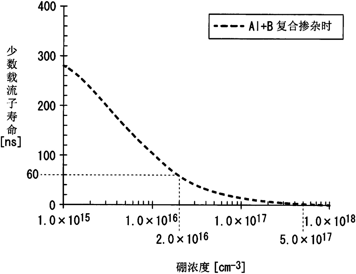
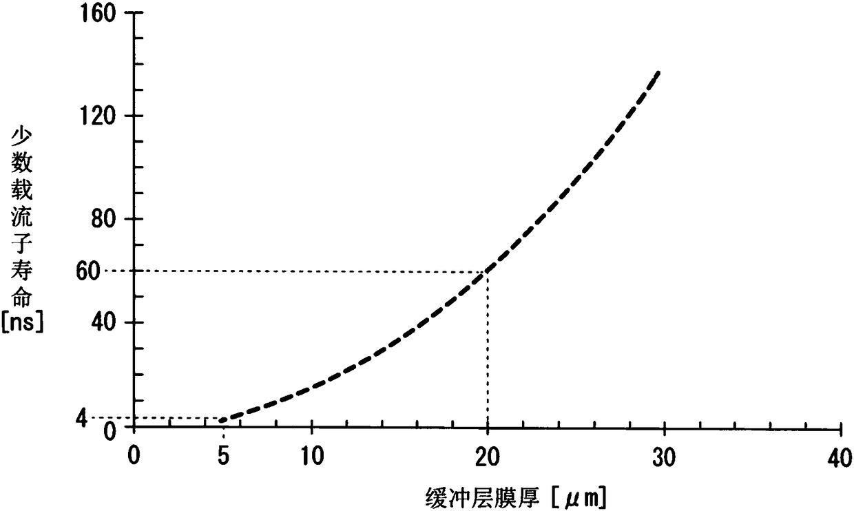
[0090] The region 2a for the p-type buffer layer has a region for the collector, and the region for the collector has a thickness t1 of 5 μm or more and 20 μm or less, in the form of 5×10 17 cm -3 Above and 5×10 18 cm -3 Al is added at the following concentration, and at 2×10 16 cm -3 More than and less than 5×10 17 cm -3 Concentrations added with B. The second SiC epitaxial wafer (1, 20, 2a, 3, 4) is also Figure 4 The shown first SiC epitaxial wafers ( 1 , 2 a , 3 , 4 ) similarly use boron added to the buffer layer to promote the capture and eliminati...
PUM
 Abstract
Description
Claims
Application Information
 - R&D
- Intellectual Property
- Life Sciences
- Materials
- Tech Scout
- Unparalleled Data Quality
- Higher Quality Content
- 60% Fewer Hallucinations
Browse by: Latest US Patents, China's latest patents, Technical Efficacy Thesaurus, Application Domain, Technology Topic, Popular Technical Reports.
© 2025 PatSnap. All rights reserved.Legal|Privacy policy|Modern Slavery Act Transparency Statement|Sitemap|About US| Contact US: help@patsnap.com