
Large-power vertical structure LED epitaxial structure and preparation method thereof
A vertical structure, epitaxial structure technology, applied in electrical components, nanotechnology, circuits, etc., can solve the problems of ohmic contact electrode difficulties, optical and electrical performance limitations, low carrier concentration, etc., to enhance current expansion, improve Photoelectric performance, wide application effect
- Summary
- Abstract
- Description
- Claims
- Application Information
AI Technical Summary
Problems solved by technology
Method used
Image

Examples
Embodiment 1
[0036] A method for preparing a high-power vertical structure LED epitaxial structure, comprising the following steps:
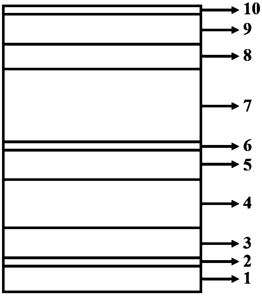
[0037] 1) Place the Si substrate 1 in the MOCVD equipment, select the (111) crystal plane of the Si substrate 1, and sequentially deposit a 2nm pre-coated Al layer 2, a 150nm thick AlN buffer layer 3, and a 500nm thick AlGaN buffer layer 4 , a u-type GaN layer 5 with a thickness of 1000nm;
[0038]Specifically, the operating parameters of the pre-laid Al layer 2: the substrate temperature is 950° C., the reaction chamber pressure is 40 Torr, the graphite disk rotation speed is 900 r / min, and the flow rate of TMAl is 250 sccm;
[0039] The operating parameters for depositing the AlN buffer layer 3: the substrate temperature is 1100° C., the reaction chamber pressure is 50 Torr, the graphite disc rotation speed is 1200 r / min, the flow rate of TMAl is 350 sccm, NH 3 The flow rate is 20slm;
[0040] The operating parameters for depositing the AlGaN buffer laye...
Embodiment 2
[0052] A method for preparing a high-power vertical structure LED epitaxial structure, comprising the following steps:
[0053] 1) Place the Si substrate 1 in the MOCVD equipment, select the (111) crystal plane of the Si substrate 1, and sequentially deposit a 2nm pre-coated Al layer 2, a 150nm thick AlN buffer layer 3, and a 500nm thick AlGaN buffer layer 4 , a u-type GaN layer 5 with a thickness of 1000nm;
[0054] Specifically, the operating parameters of the pre-laid Al layer 2: the substrate temperature is 950° C., the reaction chamber pressure is 40 Torr, the graphite disk rotation speed is 900 r / min, and the TMAl flow rate is 250 sccm;
[0055] The operating parameters for depositing the AlN buffer layer 3: the substrate temperature is 1100° C., the reaction chamber pressure is 50 Torr, the graphite disc rotation speed is 1200 r / min, the flow rate of TMAl is 350 sccm, NH 3 The flow rate is 20slm;
[0056] The operating parameters for depositing the AlGaN buffer layer ...
PUM
| Property | Measurement | Unit |
|---|---|---|
| thickness | aaaaa | aaaaa |
| thickness | aaaaa | aaaaa |
| thickness | aaaaa | aaaaa |
Abstract
Description
Claims
Application Information