Semiconductor nanocrystal and preparation method thereof
A nanocrystal and semiconductor technology, applied in nanotechnology, nano optics, nanotechnology, etc., can solve the problems of quantum dots with many steps, increase energy consumption, and affect the progress of industrialization, so as to simplify the preparation steps, reduce self-absorption, The effect of promoting progress
- Summary
- Abstract
- Description
- Claims
- Application Information
AI Technical Summary
Problems solved by technology
Method used
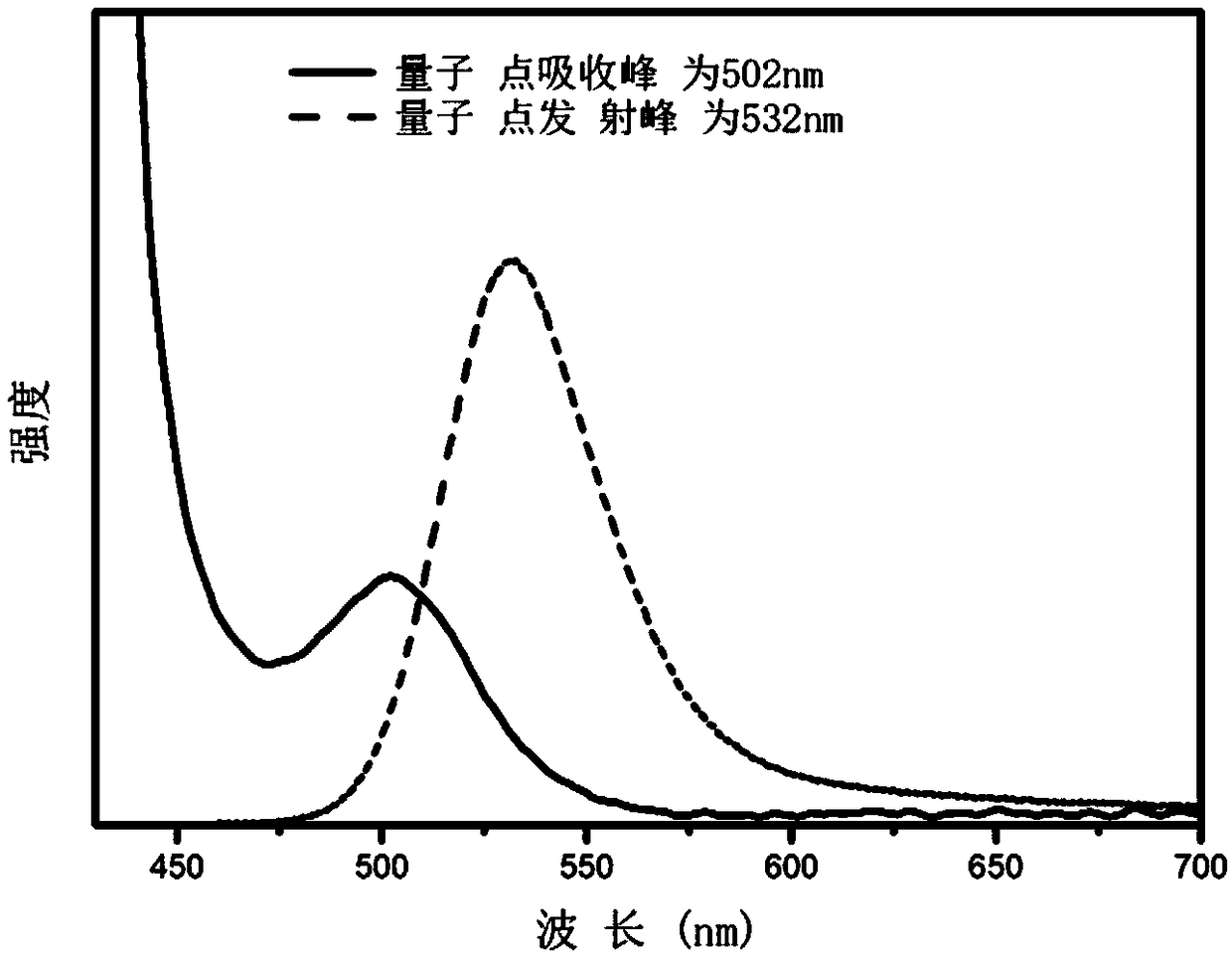
Image

Examples
preparation example Construction
[0022] A method for preparing semiconductor nanocrystals provided by an embodiment of the present invention comprises the following steps:
[0023] providing a cationic precursor solution comprising at least a first cationic precursor and a second cationic precursor;
[0024] providing an anion precursor solution comprising at least an anion precursor;
[0025] Mixing and reacting the cation precursor solution with the anion precursor solution to obtain semiconductor nanocrystals;
[0026] The structural formula of the anion precursor is (NR 1 R 2 ) 3 P=E, E includes S, Se or Te, R 1 Including hydrogen, alkyl chains with 1 to 10 carbon atoms, alkane chains with 1 to 10 carbon atoms, olefin chains with 1 to 10 carbon atoms, and 1 to 10 carbon atoms with substituents Any one or a combination of two or more of olefin chains and aromatic chains with 5 to 18 carbon atoms, R 2 Including hydrogen, alkyl chains with 1 to 10 carbon atoms, alkane chains with 1 to 10 carbon atoms, ...
Embodiment 1
[0069] Preparation of In-Zn-P-S Semiconductor Nanocrystals with Composite Structure
[0070] 1. The temperature of the In-Zn precursor is raised to 200°C under a nitrogen atmosphere;
[0071] 2. Add 0.5ml S-P(EDA) 3 solution, reacted for 30 minutes to prepare In-Zn-P-S nanocrystals.
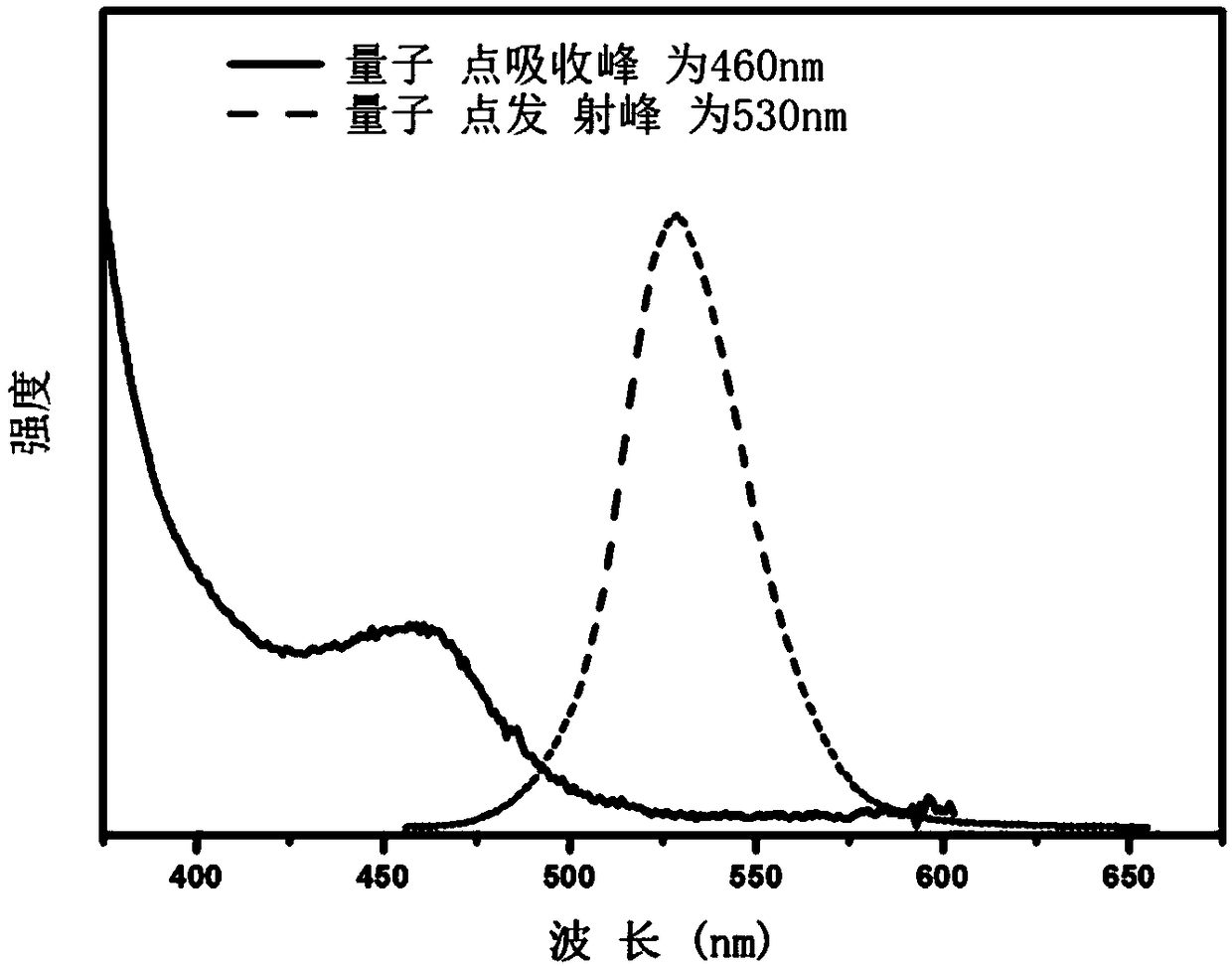
[0072] Samples were tested for their ultraviolet-visible absorption (UV-Vis) and fluorescence emission (PL) spectra.
[0073] Its absorption peak is 460nm, its fluorescence emission peak is 530nm, its half-width is 38nm, and its quantum yield is 80% when tested with an integrating sphere. Its Stokes shift is 70nm.
Embodiment 2
[0075] Preparation of Cd-Zn-P-Se Semiconductor Nanocrystals with Composite Structure
[0076] 1. The temperature of the Cd-Zn precursor is raised to 200°C under nitrogen atmosphere;
[0077] 2. Add 0.5ml Se-P(EDA) 3 solution, and reacted for 30 minutes to prepare Cd-Zn-P-Se nanocrystals.
[0078] 3 Heat up to 300°C, add 1ml of dodecanethiol (DDT), and react for 20in
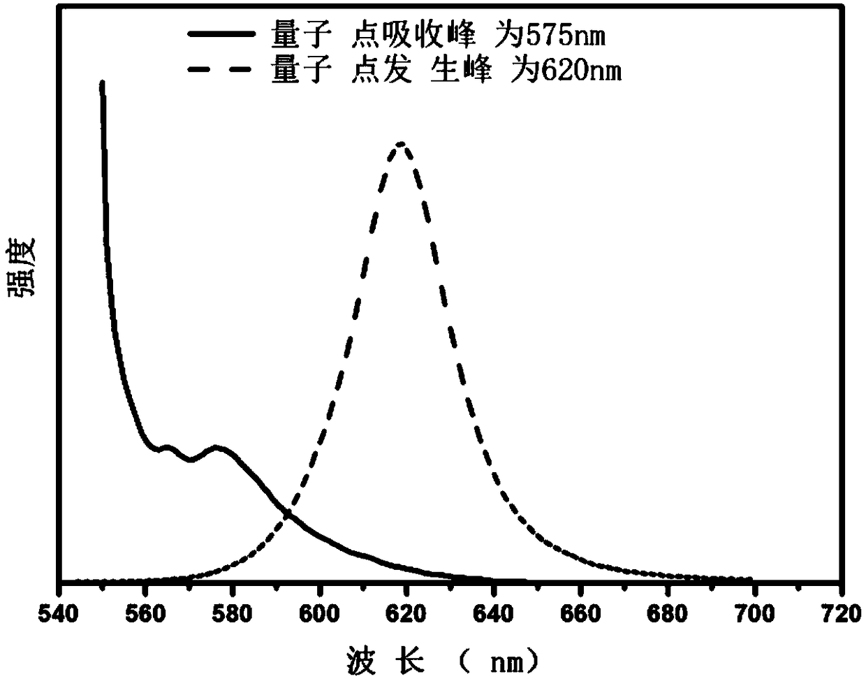
[0079] Samples were tested for their ultraviolet-visible absorption (UV-Vis) and fluorescence emission (PL) spectra.
[0080] It has an absorption peak of 575nm, a fluorescence emission peak of 620nm, a half-maximum width of 21nm, and a quantum yield of 85% when tested using an integrating sphere. Its Stokes shift is 45nm.
PUM
| Property | Measurement | Unit |
|---|---|---|
| Size | aaaaa | aaaaa |
| Half width | aaaaa | aaaaa |
| Half width | aaaaa | aaaaa |
Abstract
Description
Claims
Application Information
 - R&D Engineer
- R&D Manager
- IP Professional
- Industry Leading Data Capabilities
- Powerful AI technology
- Patent DNA Extraction
Browse by: Latest US Patents, China's latest patents, Technical Efficacy Thesaurus, Application Domain, Technology Topic.
© 2024 PatSnap. All rights reserved.Legal|Privacy policy|Modern Slavery Act Transparency Statement|Sitemap