Molybdenum disulfide-based visible near-infrared InGaAs detector and fabrication method thereof
A molybdenum disulfide and near-infrared technology, applied in the field of detectors, can solve the problems of complex detection system, inability to identify lasers, large system size and weight, etc., and achieve the effects of low preparation cost, improved light response, and simple preparation process
- Summary
- Abstract
- Description
- Claims
- Application Information
AI Technical Summary
Problems solved by technology
Method used
Image

Examples
Embodiment 1
[0028] Embodiment 1, concrete technological process is:
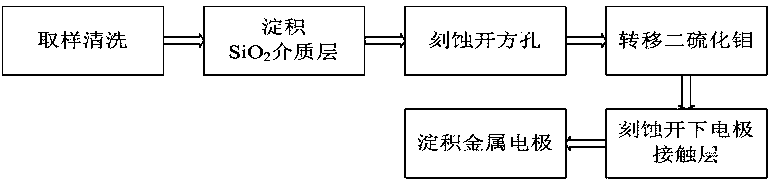
[0029] 1. Sampling and cleaning, using acetone, ethanol and deionized water to clean the sample ultrasonically for 8-3 mins;
[0030] 2. Deposit SiO 2 Dielectric layer 4, SiO with a thickness of 90 nm deposited by plasma enhanced chemical vapor deposition (PECVD) 2 For the dielectric layer, the substrate temperature is 330±20 ℃, and the RF power is 40±10 W;
[0031] 3. Etching square holes, using inductively coupled plasma (ICP) etching technology on SiO 2 A square hole is opened on the dielectric layer 4, and the etching conditions are as follows: ICP power is 1500 W, RF power is 25-50 W, cavity pressure is 9.4 mTorr, and temperature is 5 °C;
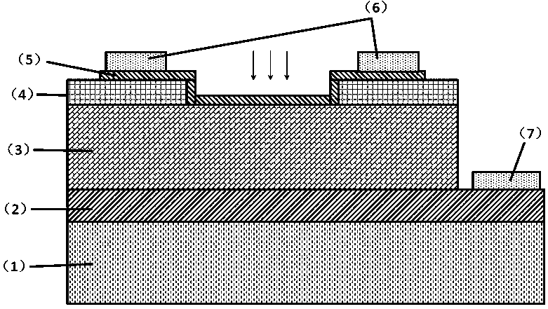
[0032] 4. Transfer molybdenum disulfide 5, using dry transfer technology, transfer the molybdenum disulfide with a layer number of one layer to the square hole, covering the entire square hole, and the molybdenum disulfide 5 is in contact with the InGaAs absorption layer 3; ...
Embodiment 2
[0035] Embodiment 2, concrete technological process is:
[0036] 1. Sampling and cleaning, using acetone, ethanol and deionized water to clean the sample ultrasonically for 8-3 mins;
[0037] 2. Deposit SiO 2 Dielectric layer 4, SiO with a thickness of 300 nm deposited by plasma enhanced chemical vapor deposition (PECVD) 2 For the dielectric layer, the substrate temperature is 330±20 ℃, and the RF power is 40±10 W;
[0038] 3. Etching square holes, using inductively coupled plasma (ICP) etching technology on SiO 2 A square hole is opened on the dielectric layer 4, and the etching conditions are as follows: ICP power is 1500 W, RF power is 25-50 W, cavity pressure is 9.4 mTorr, and temperature is 5 °C;
[0039] 4. Transfer molybdenum disulfide 5, using dry transfer technology to transfer molybdenum disulfide with 3 layers onto the square hole to cover the entire square hole, and the molybdenum disulfide 5 is in contact with the InGaAs absorption layer 3;
[0040] 5. Etching...
Embodiment 3
[0042] Embodiment 3, concrete technological process is:
[0043] 1. Sampling and cleaning, using acetone, ethanol and deionized water to clean the sample ultrasonically for 8-3 mins;
[0044] 2. Deposit SiO 2 Dielectric layer 4, SiO with a thickness of 300 nm deposited by plasma enhanced chemical vapor deposition (PECVD) 2For the dielectric layer, the substrate temperature is 330±20 ℃, and the RF power is 40±10 W;
[0045] 3. Etching square holes, using inductively coupled plasma (ICP) etching technology on SiO 2 A square hole is opened on the dielectric layer 4, and the etching conditions are as follows: ICP power is 1500 W, RF power is 25-50 W, cavity pressure is 9.4 mTorr, and temperature is 5 °C;
[0046] 4. Transfer molybdenum disulfide 5, using dry transfer technology, transfer five layers of molybdenum disulfide to the square hole, covering the entire square hole, and the molybdenum disulfide 5 is in contact with the InGaAs absorption layer 3;
[0047] 5. Etching th...
PUM
| Property | Measurement | Unit |
|---|---|---|
| thickness | aaaaa | aaaaa |
| thickness | aaaaa | aaaaa |
| thickness | aaaaa | aaaaa |
Abstract
Description
Claims
Application Information
 - R&D
- Intellectual Property
- Life Sciences
- Materials
- Tech Scout
- Unparalleled Data Quality
- Higher Quality Content
- 60% Fewer Hallucinations
Browse by: Latest US Patents, China's latest patents, Technical Efficacy Thesaurus, Application Domain, Technology Topic, Popular Technical Reports.
© 2025 PatSnap. All rights reserved.Legal|Privacy policy|Modern Slavery Act Transparency Statement|Sitemap|About US| Contact US: help@patsnap.com