A DC switching power conversion circuit with step-down and step-up functions
A technology of power conversion circuit and DC switch, which is applied in battery circuit devices, output power conversion devices, and DC power input conversion to DC power output, etc. problems, to achieve good practicability and economy, high power conversion efficiency, quick installation and maintenance
- Summary
- Abstract
- Description
- Claims
- Application Information
AI Technical Summary
Problems solved by technology
Method used
Image
Examples
Embodiment 1
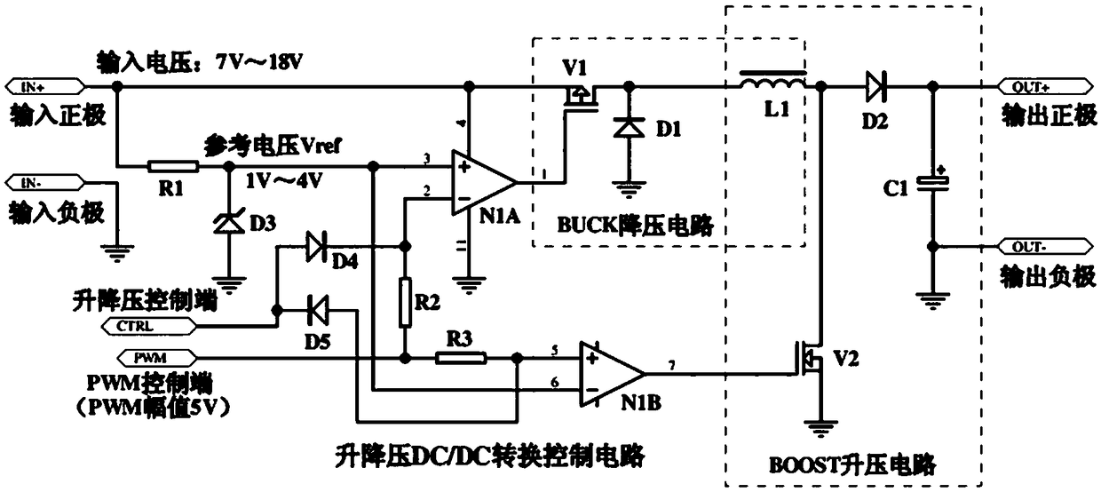
[0022] Example 1, figure 1 It is a schematic diagram of the circuit structure of the present invention.
[0023] figure 1 It shows a structural block diagram according to an embodiment of the present invention. It can be seen from the figure that a DC switching power supply conversion circuit that can be bucked or boosted includes an input positive pole, an input negative pole, a buck-boost control terminal, PWM control terminal, resistors R1-R3, diodes D1, D2, D3, D4, D5, operational amplifiers N1A, N1B, inductor L1, capacitor C1, N-channel FET V2, P-channel FET V1, positive output, output Negative pole, the diode D3 is a Zener diode, the input positive pole is connected to one end of the resistor R1, the positive power supply terminal of the operational amplifier N1A and the S pole of the field effect transistor V1; the other end of the resistor R1 is connected to the Zener diode D3 The negative pole and the positive input terminal of the operational amplifier N1A are conn...
PUM
 Abstract
Description
Claims
Application Information
