A Te/MoS2 van der Waals heterostructure and preparation method and application thereof

A heterogeneous structure, nanosheet technology, applied in the direction of final product manufacturing, sustainable manufacturing / processing, nanotechnology for materials and surface science, etc., can solve the problem of slow response speed, achieve fast response time, The effect of low cost and fast synthesis speed

Active Publication Date: 2018-12-21
THE NAT CENT FOR NANOSCI & TECH NCNST OF CHINA
View PDF5 Cites 12 Cited by
  • Summary
  • Abstract
  • Description
  • Claims
  • Application Information

AI Technical Summary

Problems solved by technology

However, the quantum dots synthesized by the hydrothermal method will bring a large number of bulk defects and interface defects, making this type of detector work in the defect-assisted photoconductive mechanism-grating mechanism, which will seriously slow down the response while obtaining high responsivity. speed

Method used


Image

  • A Te/MoS2 van der Waals heterostructure and preparation method and application thereof
  • A Te/MoS2 van der Waals heterostructure and preparation method and application thereof
  • A Te/MoS2 van der Waals heterostructure and preparation method and application thereof

Examples


Embodiment 1

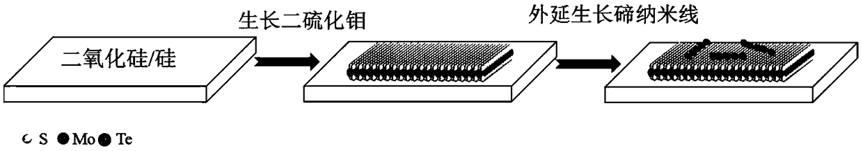
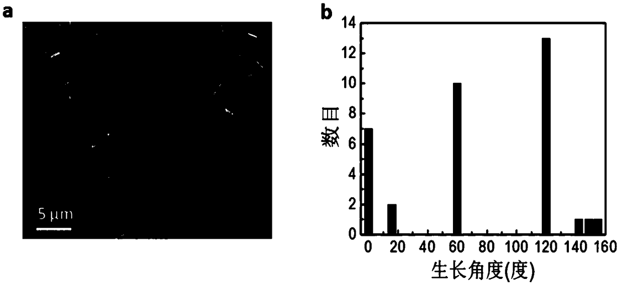
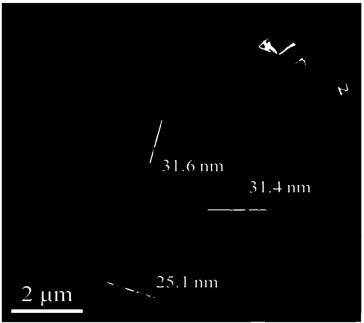
[0036] This embodiment provides a Te / MoS 2 Van der Waals heterostructures, including MoS 2 nanosheet layer and Te nanowire layer, the Te nanowire layer is epitaxially grown on the MoS 2 nanosheet surface.

[0037] This embodiment also provides the above-mentioned Te / MoS2 The preparation method of van der Waals heterostructure (its flow chart is as figure 1 shown), including the following steps:

[0038] (1) Mix hydrogen peroxide and concentrated sulfuric acid at a ratio of 1:3 by volume, put the cut silicon chip into it, heat it at 140°C for 3 hours, and then use acetone, ethanol and deionized water to sonicate for 20 minutes each, Blow dry with nitrogen;

[0039] (2) MoO 3 powder and S powder are respectively placed in the downstream central temperature zone and upstream central temperature zone of the dual temperature zone tube furnace, and the silicon wafer is placed in MoO 3 Above the powder, after cleaning the quartz tube with argon, the temperature of the downstrea...

Embodiment 2

[0057] This embodiment provides a Te / MoS 2 Van der Waals heterostructures, including MoS 2 nanosheet layer and Te nanowire layer, the Te nanowire layer is epitaxially grown on the MoS 2 nanosheet surface.

[0058] This embodiment also provides the above-mentioned Te / MoS 2 A method for preparing a van der Waals heterostructure, comprising the following steps:

[0059] (1) Mix hydrogen peroxide and concentrated sulfuric acid at a ratio of 1:3 by volume, put the cut silicon chip into it, heat it at 140°C for 3 hours, and then use acetone, ethanol and deionized water to sonicate for 20 minutes each, Blow dry with nitrogen;

[0060] (2) MoO 3 powder and S powder are respectively placed in the downstream central temperature zone and upstream central temperature zone of the dual temperature zone tube furnace, and the silicon wafer is placed in MoO 3 Above the powder, after cleaning the quartz tube with argon, the temperature of the downstream central temperature zone was raised...


PUM

PropertyMeasurementUnit
lengthaaaaaaaaaa
thicknessaaaaaaaaaa
thicknessaaaaaaaaaa

Abstract

A Te / MoS2 van der Waals heterostructure includes a MoS2 nanosheet layer and a Te nanowire layer epitaxially grown on the surface of the MoS2 nanosheet layer, and a Te nanowire layer epitaxially grownon the surface of the MoS2 nanosheet. The Van der Waals heterostructure of the present invention uses a Te nanowire with a narrow band gap and a one-dimensional structure as an infrared absorption layer and a MoS2 nanosheet with a two-dimensional structure as a conductive channel, and the structure has stable chemical properties. Applied in infrared detector, infrared detector works in photovoltaic mechanism, has good performance, and shows ultra-high responsiveness (1.9 * 103 A / W) and fast response time (Tau rising=15 ms, Tau decay=32 ms) at 1550 nm. As that Te / MoS2 van der Waals heterostructure is prepare by a physical vapor deposition method, the Te / MoS2 van der Waals heterostructure has the advantages of low cost, simple process, high synthesis speed and the like.

Description

technical field [0001] The invention relates to the technical field of inorganic semiconductor nanomaterials, in particular to a Te / MoS 2 Van der Waals heterostructures and methods for their preparation and applications. Background technique [0002] Infrared detection has very important applications in the fields of communication, thermal imaging, biological imaging and remote sensing technology. Therefore, the development of high-performance infrared detectors is an urgent need for the country in key fields such as civil and military applications. At present, silicon-based semiconductor devices commonly used have reached the limit of Moore's law. In addition, due to the band gap limitation (~1.1eV) of silicon itself, it can only absorb light with a wavelength of less than 1100nm. In order to break through the limitations of traditional silicon, it is necessary to find new material systems or device structures to improve the operating wavelength range and infrared detecti...

Claims


Application Information

Patent Timeline
Patent Type & Authority Applications(China)
IPC IPC(8): H01L31/109H01L31/0336H01L31/18B82Y40/00B82Y30/00
CPCB82Y30/00B82Y40/00H01L31/0336H01L31/109H01L31/1836Y02E10/50Y02P70/50
Inventor 何军李宁宁
Owner THE NAT CENT FOR NANOSCI & TECH NCNST OF CHINA
Why Eureka
Try Eureka