Processing method for micro-nano structure of array of ultrafast laser combined pulse sequence

An ultra-fast laser and combined pulse technology, which is applied in laser welding equipment, metal processing equipment, manufacturing tools, etc., can solve the problems of affecting processing efficiency, many micro-nano structure processes, and inability to continue, so as to improve processing efficiency and improve processing efficiency. The effect of efficiency and quality

Inactive Publication Date: 2018-12-25
GUANGDONG UNIV OF TECH
View PDF8 Cites 12 Cited by
  • Summary
  • Abstract
  • Description
  • Claims
  • Application Information

AI Technical Summary

Problems solved by technology

[0003] At present, the main technical problems in the existing technology are: 1. There are many processes in the processing of micro-nano structures, and each process cannot be continuous, which affects the processing efficiency
2. The existing processing methods are limited in the field of micro-nano structure processing of hard and brittle materials

Method used


Image

  • Processing method for micro-nano structure of array of ultrafast laser combined pulse sequence
  • Processing method for micro-nano structure of array of ultrafast laser combined pulse sequence
  • Processing method for micro-nano structure of array of ultrafast laser combined pulse sequence

Examples


Embodiment 1

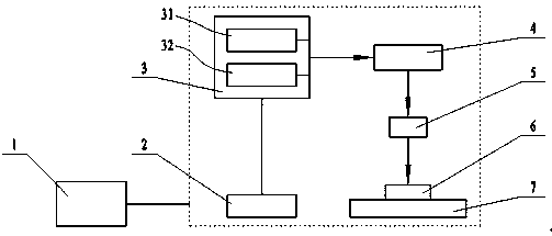
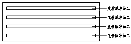
[0028] An array micro-nano structure processing method of an ultrafast laser combined pulse sequence, comprising the following steps: grinding and polishing the surface of a silicon nitride workpiece 6 to be processed, cleaning and drying it ultrasonically with alcohol, and fixing it on an ultra-precision platform 7 superior. Start the femtosecond laser 31 by the industrial control computer 1 through the laser controller 2 to emit the laser beam to the surface of the silicon nitride workpiece 6 to complete laser focusing, turn off the femtosecond laser 31, and adjust the ultra-precision platform 7 to determine the processing area of ​​the silicon nitride workpiece 6 . When the silicon nitride workpiece 6 is processed, the laser controller 2 is turned on by the industrial control computer 1 to select the femtosecond laser 31 in the laser generator 3 to emit a femtosecond pulse sequence, which is incident on the silicon nitride through the optical path switching module 4 and the...

Embodiment 2

[0030]An array micro-nano structure processing method of ultrafast laser combined pulse sequence, comprising the following steps: grinding and polishing the surface of the aluminum oxide workpiece 6 to be processed, ultrasonically cleaning and drying with acetone, and fixing it on an ultra-precision platform 7 . The industrial control computer 1 starts the picosecond laser 32 through the laser controller 2 to emit the laser beam to the surface of the alumina workpiece 6 to complete laser focusing, turns off the picosecond laser 32, and adjusts the ultra-precision platform 7 to determine the processing area of ​​the alumina workpiece 6. When the alumina workpiece 6 is processed, the industrial control computer 1 turns on the laser controller 2 to select the picosecond laser 32 in the laser generator 3 to emit a picosecond pulse sequence, which is incident on the alumina workpiece 6 through the optical path switching module 4 and the focusing module 5 in sequence. surface, and s...

Embodiment 3

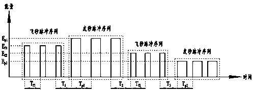
[0032] This embodiment provides an array micro-nano structure processing method of the same ultrafast laser combination pulse sequence as in Embodiment 1, the difference is that the pulse interval T of the femtosecond pulse sequence f1 40ns, pulse energy E f1 150μJ, laser scanning speed V 1 is 400mm / s, and the focus position is 1mm, the pulse interval T between the picosecond pulse sequence and the femtosecond pulse sequence 1 Pulse interval T of 150ns, picosecond pulse sequence p1 10ns, pulse energy E p1 100μJ, laser scanning speed V 2 is 1000mm / s, and the focus position is 0mm.


PUM


Abstract

The invention provides a processing method for a micro-nano structure of an array of an ultrafast laser combined pulse sequence. The processing method comprises the following steps: grinding and polishing and cleaning and drying the surface of a workpiece, and fixing the workpiece to an ultra-precision platform; starting a laser generator through a laser controller to emit a laser beam by means ofan industrial control computer and adjusting the ultra-precision platform to determine a workpiece processing region till the surface of the workpiece is focused by laser; during processing, selecting a femtosecond laser or a picosecond laser through a laser controller to emit the laser beam to achieve ultrafast laser pulse free combination through a light path switching module, and carrying outprocessing according to a needed micro-nano structure; and after processing, taking the workpiece down, and cleaning and drying the workpiece to obtain a finished product. The invention provides a novel combination mode of a laser processing process in micro-nano material processing. Femtosecond laser or picoseconds laser can be selected according to the processing demand, and an ultrafast laser pulse sequence can be combined flexibly by way of light path switching, so that the processing efficiency and quality of the micro-nano structure are improved effectively.

Description

technical field [0001] The invention belongs to the technical field of laser processing, and in particular relates to an array micro-nano structure processing method of an ultrafast laser combined pulse sequence. Background technique [0002] The micro-nano structure on the surface of the material enables the material to exhibit its inherent properties while having properties that conventional surfaces do not have, such as hydrophobicity, anti-friction, and antibacterial properties. It has been widely used in the manufacture of functional parts. The micro-nano structure has a great influence on the surface properties of materials, and can be prepared by chemical etching, vapor deposition, laser processing and other methods. Due to its good mechanical and physical and chemical properties, ceramics are an important research field for micro-nano structure processing. As a typical hard and brittle material, the laser processing method with non-contact, no tool wear, high effi...

Claims


Application Information

Patent Timeline
Patent Type & Authority Applications(China)
IPC IPC(8): B23K26/00B23K26/04B23K26/06
CPCB23K26/04B23K26/0604
Inventor 王成勇王宏建林华泰
Owner GUANGDONG UNIV OF TECH
Why Eureka
Try Eureka