
Large dynamic range weak light detection system based on avalanche photodiode array chip

A diode array and photodiode technology, which is applied in the field of photoelectric detection, can solve the problems of increasing the detection time of the system, requiring a long time for adjustment, and limiting the dynamic range of the detection system.

Active Publication Date: 2018-12-28
传周半导体科技(上海)有限公司
View PDF8 Cites 19 Cited by
  • Summary
  • Abstract
  • Description
  • Claims
  • Application Information

AI Technical Summary

Problems solved by technology

[0006] 1. The avalanche photodiode used only works in one mode (linear mode or single photon detection mode), which makes the detection system unable to perform effective photoelectric conversion from single photon level to strong optical signal, which limits the dynamic range of the detection system
[0007] 2. The detection speed of the system is greatly limited
During the detection process, the reverse bias voltage of the avalanche diode needs to be adjusted several times, and since the avalanche diode is generally biased at a higher voltage and requires a very small bias voltage ripple, the bias voltage output terminal will generally be A variety of filters are added to reduce noise, which will take a long time for the system to adjust the bias voltage
In addition, the feedback system needs to identify, calculate and judge the measured signal during the bias adjustment process, which further increases the system detection time
It can be seen from the above that the detection speed of the system will be greatly affected, which limits its application in continuous optical signal detection and fast photoelectric detection systems
For example, in the fluorescence detection system that avalanche photodiodes are often used in, in order to reduce the influence of photobleaching (also known as photobleaching, photobleaching) and avoid photochemical damage to fluorophores, the exposure and detection times are generally very short. The design described above obviously cannot be applied in this field

Method used


Image

  • Large dynamic range weak light detection system based on avalanche photodiode array chip
  • Large dynamic range weak light detection system based on avalanche photodiode array chip
  • Large dynamic range weak light detection system based on avalanche photodiode array chip

Examples


Embodiment Construction

[0025] The present invention will be further described below in conjunction with specific examples.

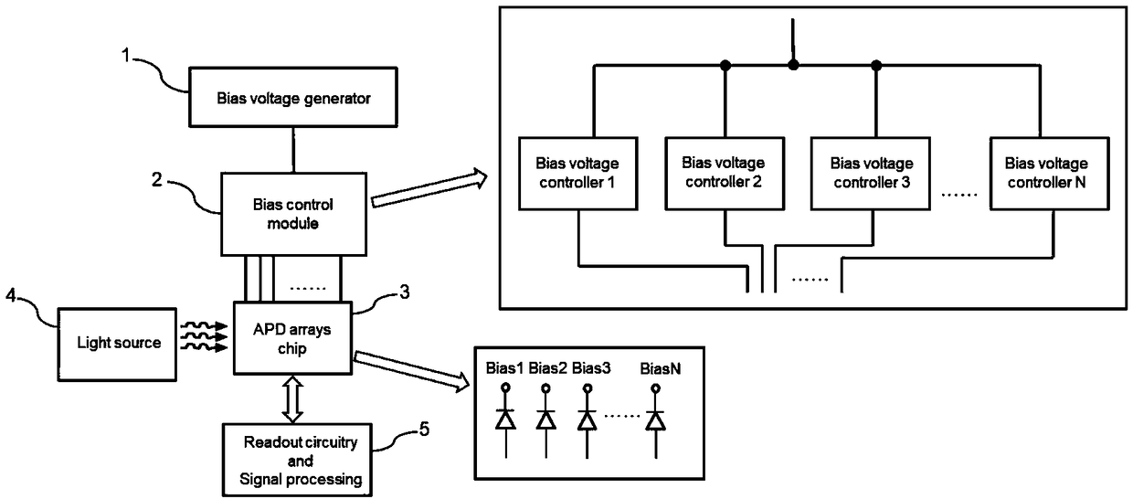
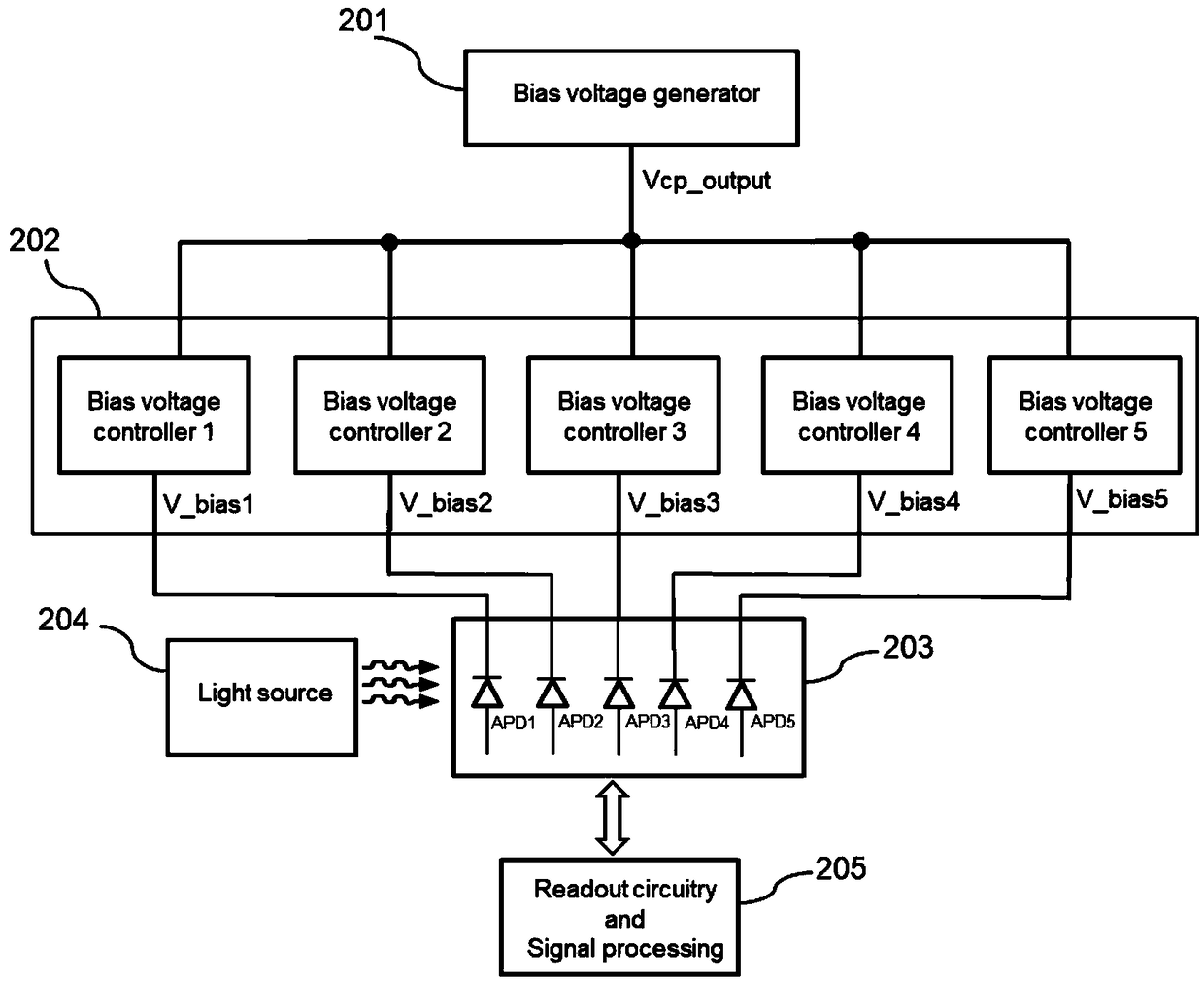
[0026] figure 2 An embodiment of a large dynamic range weak light detection system based on an avalanche photodiode array chip and its bias voltage control circuit is given. The system is composed of a bias voltage generator module 201 , a bias voltage control module 202 , an avalanche photodiode array chip 203 , a light source 204 , and a signal readout and processing system 205 . The bias voltage generator module 201 produces high voltage (Vcp_output), and outputs the required bias voltage of each photodiode in the avalanche photodiode array chip 203 through the bias voltage control module 202, and the bias voltage control module 202 has 5 output control modules respectively Used to control the output voltages Vbias1-Vbias5, the number of output voltages is the same as the number of avalanche photodiodes in the avalanche photodiode array chip 3; the avalanche photodiodes i...


PUM


Abstract

The invention provides a large dynamic range weak light detection system based on an avalanche photodiode array chip. The large dynamic range weak light detection system consists of a bias generator module 1, a bias control module 2, an avalanche photodiode array chip 3, a light source 4, and a signal readout and processing module 5. The large dynamic range weak light detection system provided bythe invention can be widely used in the fields of extremely weak light measurement such as laser ranging, DNA sequencing, quantum key distribution, laser radar, medical imaging, etc.

Description

(1) Technical field [0001] The invention relates to a large dynamic range weak light detection system based on an avalanche photodiode array chip, which can be used for extremely weak light measurement such as laser ranging, DNA sequencing, quantum key distribution, laser radar and medical imaging and other applications. It belongs to the technical field of photoelectric detection. (2) Background technology [0002] The avalanche photodiode is a semiconductor photodetector. When it is running, a higher reverse bias voltage is applied to it, and a larger gain can be obtained internally by using its internal avalanche breakdown effect. When the reverse bias voltage is lower than its breakdown voltage, the avalanche photodiode works in the linear region, and the internal gain is generally tens to 10 3 ; When the reverse bias voltage is higher than its breakdown voltage, the avalanche photodiode works in Geiger mode (also known as single photon mode), and the internal gain can ...

Claims


Application Information

Patent Timeline
IPC IPC(8): G01J1/42G01J1/44
CPCG01J1/4228G01J1/44G01J2001/4466
Inventor 邓仕杰张文涛苑立波
Owner 传周半导体科技(上海)有限公司
Learn More