A light emit diode having a uniform electrode electric field distribution and a method for manufacture that same

A technology of light-emitting diodes and electric field distribution, which is applied in the direction of circuits, electrical components, semiconductor devices, etc., can solve the problems that the improvement of the electric field at the edge of the electrode has no obvious effect, the improvement of the electric field at the edge of the electrode has no effect, and the distribution of the electric field of the electrode has not been mentioned, etc., to achieve relief Current crowding effect, improvement of light extraction efficiency, effect of weakening current crowding effect

Pending Publication Date: 2019-01-04
HEBEI UNIV OF TECH
View PDF7 Cites 1 Cited by
  • Summary
  • Abstract
  • Description
  • Claims
  • Application Information

AI Technical Summary

Problems solved by technology

Although the above two structures slow down the current crowding effect to a certain extent, the influence on the electric field distribution of the electrodes is not mentioned
For the first SiO2 electron blocking layer structure, the SiO2 structure is located between the current spreading layer and the P-type transport layer to improve the current distribution. This structure has no obvious effect on the improvement of the electric field at the edge of the electrode; for the second P Extremely ohmic contact layer structure, palladium is a noble metal, and the metal embedded in the metal electrode has no effect on improving the electric field at the edge of the electrode, and additional noble metal materials also increase the production cost

Method used


Image

  • A light emit diode having a uniform electrode electric field distribution and a method for manufacture that same
  • A light emit diode having a uniform electrode electric field distribution and a method for manufacture that same
  • A light emit diode having a uniform electrode electric field distribution and a method for manufacture that same

Examples


Embodiment 1

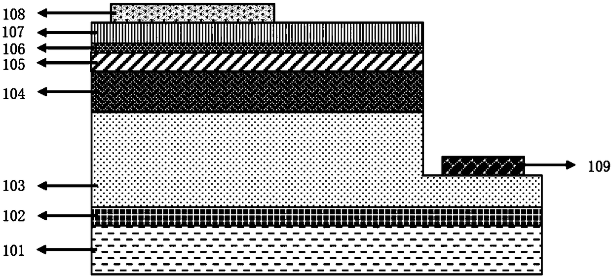
[0060] The light-emitting diode device with uniform electrode electric field distribution of this embodiment is such as Figure 7 As shown, along the epitaxial growth direction, it includes: epitaxial layer (substrate 101, buffer layer 102, N-type semiconductor transport layer 103, multiple quantum well layer 104, P-type semiconductor transport layer 105, P-type heavily doped semiconductor transport layer 106, current spreading layer 107), the N-type semiconductor transport layer 103 is partially exposed, and N-type ohmic electrodes 109 are distributed on the exposed N-type semiconductor transport layer 103; the current spreading layer 107 is distributed with The insulator layer 110 is covered with a P-type ohmic electrode 108; the insulating layer 110 is patterned with holes of the same size, and the thickness is 5nm; the P-type ohmic electrode 108 is divided into two parts , the lower part is distributed with columnar patterned electrodes matching the holes on the insulating...

Embodiment 2

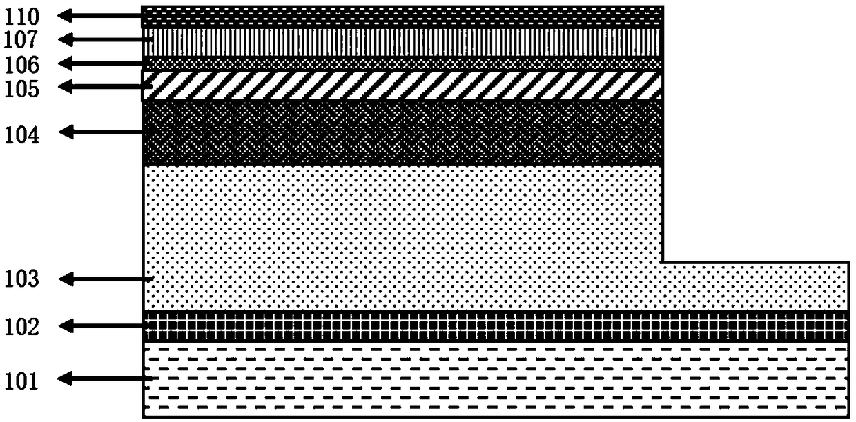
[0073] The light-emitting diode device with uniform electrode electric field distribution of this embodiment is such as Figure 7 As shown, along the epitaxial growth direction, it includes: epitaxial layers (substrate 101, buffer layer 102, N-type semiconductor transport layer 103, multiple quantum well layer 104, P-type semiconductor transport layer 105, P-type heavily doped semiconductor transport layer 106, current spreading layer 107), the N-type semiconductor transport layer 103 is partially exposed, and N-type ohmic electrodes 109 are distributed on the exposed N-type semiconductor transport layer 103; the current spreading layer 107 is distributed with The insulator layer 110 is covered with a P-type ohmic electrode 108; the insulating layer 110 is patterned with holes of the same size, and the thickness is 5nm; the P-type ohmic electrode 108 is divided into two parts , the lower part is distributed with columnar patterned electrodes matching the holes on the insulatin...

Embodiment 3

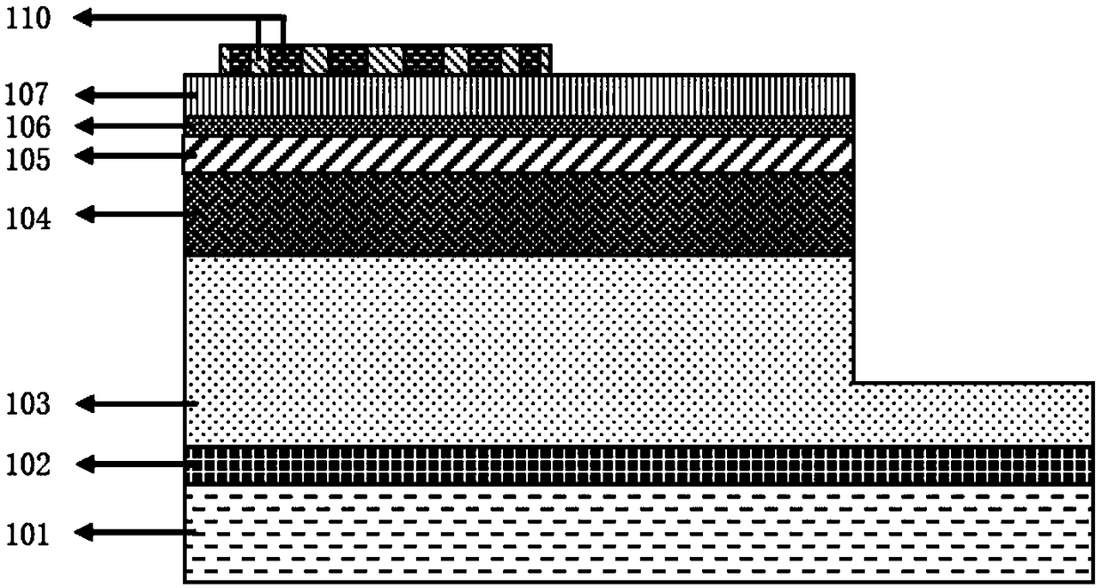
[0086] The material used in addition to the current spreading layer 107 is graphene; the insulator layer 110 first photoetches a cylindrical hole with a radius of 40 μm in the middle, and then photoetches a circle of cylindrical holes on the edge of the insulator layer 110, and every two cylindrical holes on the edge The distance between them is 200nm, the radius is 9.9μm, and the distance from the central cylindrical hole is 200nm (top view as Figure 9 ), other with embodiment 1.


PUM


Abstract

The invention relates to a light emitting diode with uniform electrode electric field distribution and a preparation method thereof. The diode comprises a substrate, a buffer layer, N-Type semiconductor transport layer, multiple quantum well layer, P-Type semiconductor transport layer, P-Type heavily doped semiconductor transport layer, current spreading layer; The N-type semiconductor transmission layer is partially exposed, and the exposed N-type semiconductor transmission layer is distributed with an N-type ohmic electrode;; An insulator layer is distributed on the current spreading layer,and the insulator layer is covered with P-Type - ohmic electrode; Holes of the same size are patterned distributed on the insulating layer; Said P-type ohmic electrode is divided into two parts, a column pattern electrode matching the holes in the insulating layer is distributed at the lower part, and an integral layered structure is arranged at the upper part, which is covered on the insulating layer. The structure of the invention improves the electric field distribution of the electrode and solves the problem of current crowding after the electric field distribution of the electrode is uniform.

Description

technical field [0001] The invention relates to the technical field of light-emitting diode semiconductors, in particular to a light-emitting diode device with uniform electrode electric field distribution and a preparation method thereof. Background technique [0002] Wide bandgap semiconductor materials (bandgap greater than or equal to 2.3eV) are called third-generation semiconductor materials, mainly including SiC, GaN, etc. Compared with the first-generation and second-generation semiconductor materials, the third-generation semiconductor materials have the characteristics of wider band gap, higher breakdown electric field, thermal conductivity and greater electron drift saturation velocity. These characteristics have led to the rapid development of nitride LED light-emitting diodes in optoelectronic devices in the blue, green and ultraviolet bands in recent years, and are widely used in lighting detection, medical phototherapy, sterilization, chemical catalysis and oth...

Claims


Application Information

Patent Timeline
Patent Type & Authority Applications(China)
IPC IPC(8): H01L33/14H01L33/38H01L33/00
CPCH01L33/007H01L33/14H01L33/38
Inventor 张勇辉郑羽欣车佳漭张紫辉
Owner HEBEI UNIV OF TECH
Why Eureka
Try Eureka