Gold sputtering target
A gold sputtering and sputtering target technology, which is applied in the field of gold sputtering targets, can solve problems such as the influence of Au film frequency characteristics, and achieve the effect of excellent uniformity and good reproducibility of film thickness distribution
- Summary
- Abstract
- Description
- Claims
- Application Information
AI Technical Summary
Problems solved by technology
Method used
Image

Examples
Embodiment 1
[0046] First, an Au block is inserted into a graphite crucible and melted. The Au melt was cast in a graphite mold to produce an Au ingot. The surface of the Au ingot was removed by grinding, and an Au blank (99.99% of purity) having a width of 190 mm, a length of 270 mm, and a thickness of 50 mm was produced. Next, the Au blank was hot-forged at a temperature of 800° C. to produce an Au target raw material with a width of 70 mm, a length of 200 mm, and a thickness of 45 mm. The machining rate during forging was set to 80% in all three axial directions. The forged Au target material was heat-treated at a temperature of 500° C. for 30 minutes. The heat-treated Au target material was ground to produce a disc-shaped Au sputtering target with a diameter of 152.4 mm and a thickness of 5 mm. Two Au sputtering targets were produced for the measurement of the characteristics of each part and the measurement of the film thickness characteristics. The same applies to the following e...
Embodiment 2~5、 comparative example 1~2
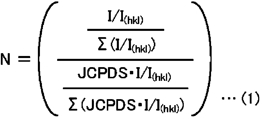
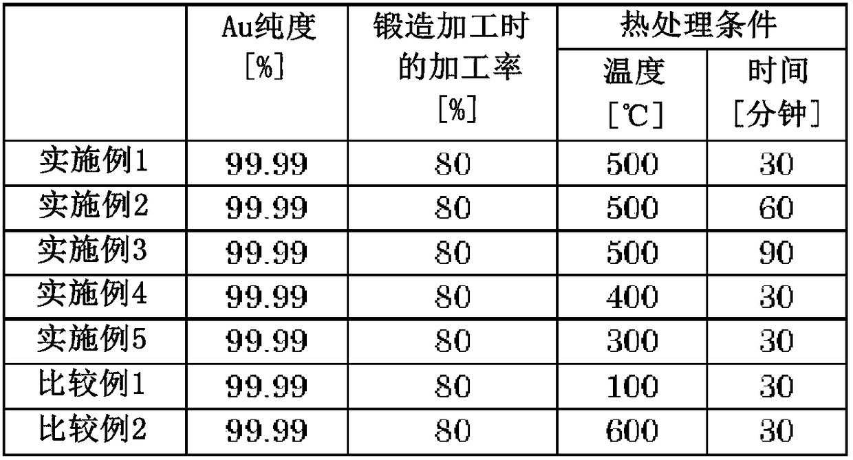
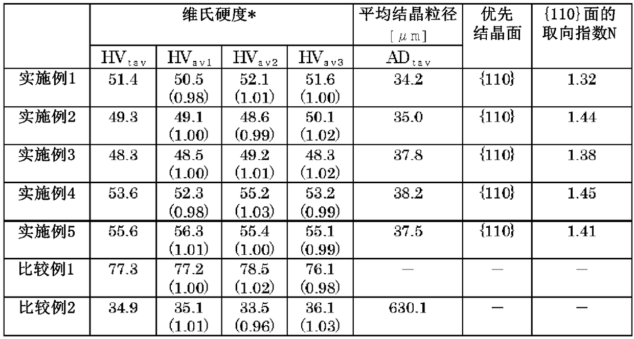
[0050] Except having applied the processing rate shown in Table 1 using the Au blank produced similarly to Example 1, it performed the forging process similarly to Example 1, and produced the Au target raw material. Next, the forged Au target material was heat-treated under the conditions shown in Table 1. Then, the Au sputtering target of the same shape as Example 1 was produced by grinding the heat-treated Au target raw material. The Vickers hardness of these Au sputtering targets, the average grain size, the preferential orientation plane of a sputtering surface, and the orientation index N of a {110} plane were measured and evaluated similarly to Example 1. These measurement results are shown in Table 2. Such an Au sputtering target was subjected to a film-forming step described later, and its characteristics were evaluated.
[0051] [Table 1]
[0052]
[0053] [Table 2]
[0054]
[0055] *Values in parentheses are relative to HV tav ratio.
[0056] The Au sp...
Embodiment 6~10
[0061] Except having applied the processing rate shown in Table 4 using the Au blank produced similarly to Example 1, it performed the forging process similarly to Example 1, and produced the Au target raw material. Next, the forged Au target material was heat-treated under the conditions shown in Table 4. Then, the Au sputtering target of the same shape as Example 1 was produced by grinding the heat-treated Au target raw material.
[0062] [Table 4]
[0063]
[0064] The Vickers hardness of the obtained Au sputtering target was measured similarly to Example 1. In addition, the average crystal grain diameter of the Au sputtering target was measured according to the measuring method of the said plate-shaped sputtering target. As a result of the measurement, the average grain size (AD) of the sputtered surface, the first section, and the second section av1 、AD av2 、AD av3 ), the average value of the above values (the average crystal grain size based on the target as a ...
PUM
| Property | Measurement | Unit |
|---|---|---|
| Vickers hardness | aaaaa | aaaaa |
| Vickers hardness | aaaaa | aaaaa |
| Vickers hardness | aaaaa | aaaaa |
Abstract
Description
Claims
Application Information
 - R&D
- Intellectual Property
- Life Sciences
- Materials
- Tech Scout
- Unparalleled Data Quality
- Higher Quality Content
- 60% Fewer Hallucinations
Browse by: Latest US Patents, China's latest patents, Technical Efficacy Thesaurus, Application Domain, Technology Topic, Popular Technical Reports.
© 2025 PatSnap. All rights reserved.Legal|Privacy policy|Modern Slavery Act Transparency Statement|Sitemap|About US| Contact US: help@patsnap.com