
Planar optical waveguide, preparation method thereof and thermo-optical device

A technology of planar optical waveguide and thermo-optic coefficient, which is applied in the field of optical waveguide, can solve the problems of no mature mechanism, slow response of optical waveguide, and insufficient sensitivity of optical waveguide thermo-optic device response, etc., to reduce thermo-optic response time, improve response speed and The effect of sensitivity

Active Publication Date: 2019-01-18
吉光半导体科技有限公司
View PDF4 Cites 4 Cited by
  • Summary
  • Abstract
  • Description
  • Claims
  • Application Information

AI Technical Summary

Problems solved by technology

[0005] Although the inorganic-organic hybrid system waveguide is conducive to the comprehensive utilization of the advantages of the two types of materials, it is not enough to combine the inorganic material system and the organic material system arbitrarily. Various complex factors such as the mutual applicability and matching between materials affect the inorganic Whether the waveguide of the organic hybrid system can be successfully developed and whether it can exert excellent thermo-optic performance, but there is no mature mechanism for how the combination of inorganic and organic materials affects the optical waveguide
[0006] At present, the organic-inorganic hybrid material system mainly uses inorganic materials as the lower cladding, and polymers as the core and upper cladding, such as SiO 2 The lower cladding layer-SU8 core layer-PMMA upper cladding layer, and this organic-inorganic hybrid material optical waveguide does not give full play to the advantages of inorganic materials and polymer materials in thermal conductivity, thermo-optic coefficient, etc., so that the response of the optical waveguide Slower, resulting in less sensitive response of optical waveguide thermo-optical devices
In addition, it requires a high-temperature process to prepare the lower cladding layer. On the one hand, the additional temperature stress will cause fractures when the grown film is too thick; on the other hand, when the temperature is higher than the heat-resistant temperature of the material, the material will begin to decompose, which will cause Device performance is unstable or even damaged

Method used


Image

  • Planar optical waveguide, preparation method thereof and thermo-optical device
  • Planar optical waveguide, preparation method thereof and thermo-optical device
  • Planar optical waveguide, preparation method thereof and thermo-optical device

Examples


preparation example Construction

[0055] The present invention also provides a method for preparing the planar optical waveguide described in the above technical solution, including:

[0056] a) growing an inorganic material lower cladding layer on the substrate surface by using a liquid phase source deposition method;

[0057] b) etching the polymer core layer on the cladding surface under the inorganic material;

[0058] c) growing an inorganic material cladding layer on the surface of the polymer core layer by using a liquid phase source deposition method;

[0059] In the step a), the deposition temperature of the liquid phase source deposition method is 80-120°C;

[0060] In the step c), the deposition temperature of the liquid phase source deposition method is 80-120°C.

[0061] According to the present invention, the lower cladding layer of inorganic material is grown on the surface of the substrate by using the liquid phase source deposition method.

[0062] In the present invention, cleaning is pref...

Embodiment 1

[0073] SiO 2 Lower cladding layer-SU-8 core layer-SiO 2 Fabrication of Overclad Ridge Optical Waveguide

[0074] see Figure 5 , Figure 5 It is a flow chart of the preparation of the ridge optical waveguide in Example 1, and the specific process is as follows:

[0075] S11: cleaning the silicon-based substrate 5 . Wash with acetone, methanol, and isopropanol in a 55°C water bath for 5 minutes, rinse the substrate (thickness: 200 μm) with deionized water and dry it under nitrogen; again use acetone, methanol, and isopropanol in a 55°C water bath Rinse the substrate with deionized water for 10 min, blow dry it under nitrogen, and heat it on a hot plate at 100°C for 10 min to dry the water vapor.

[0076] S12: Growing SiO 2 Lower cladding 6. Deposition of zero-stress SiO on substrate 5 by liquid source deposition equipment LS-CVD 2 The film is 3 μm, and the deposition temperature is 80-120°C.

[0077] Fabrication of the ridge waveguide core:

[0078] S13: Prepare the f...

Embodiment 2

[0091] The thermal-optical response characteristics of the optical waveguides of Example 1 and Comparative Examples 1-2 were detected respectively (tested by Gwinstek AFG-3081 function generator and Tektronix MSO4104B signal generator), and the test results were as follows: Figure 11 as shown, Figure 11 It is the thermo-optic response characteristic detection result figure of embodiment 2; Wherein, curve 1 is the thermo-optic response curve of the optical waveguide obtained in embodiment 1, curve 2 is the thermo-optic response curve of the optical waveguide obtained in comparative example 1, and curve 3 is the comparative example 2 Thermo-optic response curve of the obtained optical waveguide. It can be seen that the rise time t of Comparative Example 1 r_PMMA-PMMA 327μs, fall time t f_PMMA-PMMA is 327μs. Rise time t of comparative example 2 f_PMMA-Silica 196µs, fall time t f_PMMA-Silica is 163μs. The rise time t of Example 1 r_Silica-Silica 168µs, fall time t f_Sili...


PUM

PropertyMeasurementUnit
thicknessaaaaaaaaaa
thicknessaaaaaaaaaa

Abstract

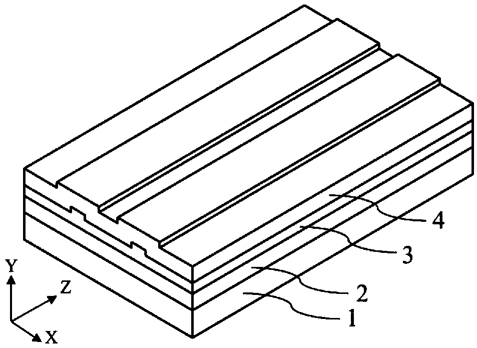
The invention provides a planar optical waveguide, a preparation method thereof and a thermo-optical device. The planar optical waveguide provided by the invention comprises substrate-inorganic material lower cladding-polymer core layer-inorganic material upper cladding, that is, the upper and lower claddings are both made of inorganic materials, and the core layer is a polymer and respectively controls the refractive indexes, thermo-optic coefficients and thermal conductivities of the inorganic material lower cladding, the polymer core layer and the inorganic material upper cladding to obtaina specific relationship of size, so that the optical field is effectively limited in the core layer by fully utilizing the characteristics such as thermal light and thermal conductivity of the inorganic material and the polymer, and the rate of change of the effective refractive index of the entire optical waveguide can be increased, thereby changing the phase of the optical field. The improvement of the characteristics of the above aspects can further effectively reduce the response time of the thermal light, improve the response speed, improve the response sensitivity of thermo-optical device, and is of great significance for obtaining a fast thermo-optical device.

Description

technical field [0001] The invention relates to the field of optical waveguide technology, in particular to a planar optical waveguide, a preparation method thereof and a thermo-optical device. Background technique [0002] An optical waveguide is a dielectric device that guides light waves to propagate in it, also known as a dielectric optical waveguide, which is a guiding structure that transmits optical frequency electromagnetic waves composed of transparent media. The transmission principle of an optical waveguide is different from that of a metal-enclosed waveguide. On the interface of media with different refractive indices, the phenomenon of total reflection of electromagnetic waves confines the light wave to the waveguide and its surrounding limited area. The optical waveguide itself is a multi-faceted scientific integration, so its research and application range is also very wide. The small and compact waveguide structure is conducive to the integration of optical c...

Claims


Application Information

Patent Timeline
Patent Type & Authority Applications(China)
IPC IPC(8): G02B6/122G02B6/132G02B6/136G02F1/01
CPCG02B6/1221G02B6/132G02B6/136G02F1/0147
Inventor 梁磊王彪张星秦莉陈泳屹陈超吴昊贾鹏张建伟周寅利曾玉刚王玉冰宁永强王立军
Owner 吉光半导体科技有限公司
Learn More