A kind of manufacturing method of white light led chip

A technology of LED chip and manufacturing method, applied in semiconductor devices, electrical components, circuits, etc., can solve the problems of poor color reproduction, low excitation efficiency, and inability to achieve high power density of white LEDs

Active Publication Date: 2020-10-27
FOSHAN EVERCORE OPTOELECTRONICS TECH
View PDF4 Cites 0 Cited by
  • Summary
  • Abstract
  • Description
  • Claims
  • Application Information

AI Technical Summary

Problems solved by technology

The silica gel in this method has low temperature resistance, so the power density of white light LEDs cannot be increased
[0004] Another way is to package red, green and blue chips inside the device together to form white light. However, the LED formed in this way has high cost, low excitation efficiency, discontinuous wavelength, and poor color reproduction. and other shortcomings

Method used


Image

  • A kind of manufacturing method of white light led chip
  • A kind of manufacturing method of white light led chip
  • A kind of manufacturing method of white light led chip

Examples


Embodiment 1

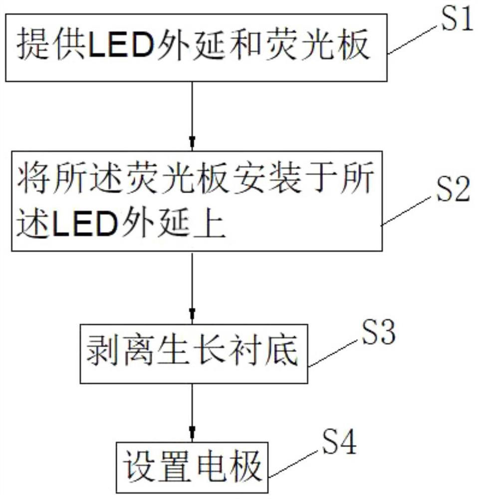
[0054] Such as Figure 1-2 Shown, a kind of manufacturing method of white light LED chip comprises the following steps:

[0055] S1. Provide an LED epitaxy 1 and a phosphor plate 2, the LED epitaxy 1 includes a growth substrate 11 and a light-emitting layer 12 grown on the growth substrate 11, wherein the light-emitting layer 12 includes N-GaN layers 121 arranged in sequence , a quantum well layer 122 and a P-GaN layer 123, wherein the N-GaN layer 121 is connected to the growth substrate 11.

[0056] The growth substrate 11 is one of a sapphire substrate, a silicon carbide substrate, a silicon substrate or a gallium nitride substrate, and the growth substrate is selected according to actual needs.

[0057]Wherein, the fluorescent plate 2 is formed by mixing fluorescent powder and a transparent high-temperature-resistant material. Specifically, the transparent high-temperature-resistant material is sapphire, glass, quartz crystal or silicon carbide. The phosphor is one or mor...

Embodiment 2

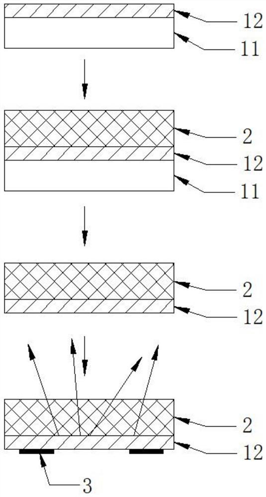
[0065] Such as Figure 3-5 As shown, this embodiment, as an improved implementation of the first embodiment, solves the problem that the luminous efficiency and the light uniformity of the white LED chip cannot be maximized.

[0066] A method for manufacturing a white light LED chip, comprising the following steps:

[0067] S1. Provide an LED epitaxy 1 and a phosphor plate 2, the LED epitaxy 1 includes a growth substrate 11 and a light-emitting layer 12 grown on the growth substrate 11, wherein the light-emitting layer 12 includes N-GaN layers 121 arranged in sequence , a quantum well layer 122 and a P-GaN layer 123, wherein the N-GaN layer 121 is connected to the growth substrate 11.

[0068] The growth substrate 11 is one of a sapphire substrate, a silicon carbide substrate, a silicon substrate or a gallium nitride substrate, and the growth substrate is selected according to actual needs.

[0069] Wherein, the fluorescent plate 2 is formed by mixing fluorescent powder and ...

Embodiment 3

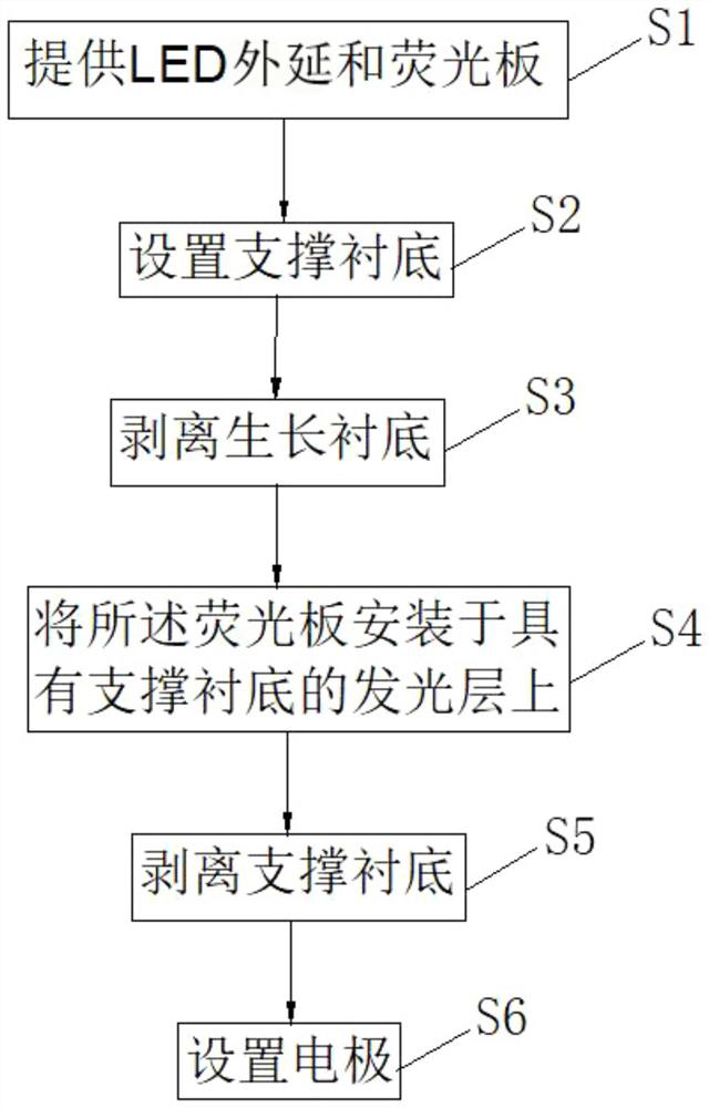
[0078] Such as Figure 6-7 As shown, this embodiment serves as an improved implementation of the above-mentioned embodiment, and solves the problem of low production efficiency of white light LED chips.

[0079] A method for manufacturing a white light LED chip, comprising the following steps:

[0080] S1. Provide an LED wafer 5 and a phosphor plate 2, the LED wafer 5 includes a growth substrate 51, a light emitting layer 52, an ohmic contact layer 53, an insulating layer 53, and an electrode layer 55 arranged in sequence, wherein the light emitting layer The number of 52 is at least one, which includes an N-GaN layer, a quantum well layer and a P-GaN layer arranged in sequence, wherein the N-GaN layer is connected to the growth substrate.

[0081] The growth substrate 51 is one of a sapphire substrate, a silicon carbide substrate, a silicon substrate or a gallium nitride substrate, and the growth substrate is selected according to actual needs.

[0082] Wherein, the fluores...


PUM


Abstract

The invention relates to a manufacturing method of a white light LED chip, comprising the following steps: S1, providing an LED epitaxial and fluorescent plate; 2, mounting that fluorescent plate on the LED epitaxy to obtain a white LED epitaxy with a growth substrate; 3, stripping that growth substrate to obtain white LED epitaxy to be formed; S4, arranging an electrode- to obtain a molded whiteLED chip. The invention provides a white LED epitaxial manufacturing method, The LED epitaxial light-emitting layer is mounted on the fluorescent plate, and the formed white LED chip can emit white light directly, and the fluorescent plate is made of high-temperature resistant transparent material and fluorescent powder, and the high-temperature generated in the working process will not affect thereliability of the fluorescent plate, and the LED chip can be made into high-power LED chip. On the other hand, the luminescence principle of the white light LED chip is that the monochromatic lightLED chip excites phosphor to form white light, the production cost is low, the package is not needed, the excitation efficiency is high, the wavelength is continuous, and the color reducibility is high.

Description

technical field [0001] The invention relates to the technical field of LED packaging, in particular to a method for manufacturing a white LED chip. Background technique [0002] With the continuous development of LED technology, the application of LED white light lighting is becoming more and more extensive, and the existing LED chip excites monochromatic light, so how to better convert the monochromatic light emitted by the LED chip into white light has always been a challenge. It is the key core technology in the field of LED. [0003] At present, there are two main ways to realize white light LED in the market: one is to select monochromatic LED chip, then mix phosphor powder and silica gel, encapsulate it on the surface of the anti-color LED chip, and excite it through the light emitted by the LED chip. Phosphor, forming white light. The silica gel in this method has low temperature resistance, so the power density of the white light LED cannot be made high. [0004] ...

Claims


Application Information

Patent Timeline
Patent Type & Authority Patents(China)
IPC IPC(8): H01L33/00H01L33/50
CPCH01L33/50H01L33/505H01L2933/0041H01L33/0093
Inventor 王孟源曾伟强董挺波
Owner FOSHAN EVERCORE OPTOELECTRONICS TECH
Why Eureka
Try Eureka