QLED device and preparation method thereof
A device and fossil technology, applied in the field of QLED devices and their preparation, can solve the problems of easily damaged quantum dot light-emitting layer, poor film-forming uniformity, uneven device light-emitting, etc., to achieve excellent light-emitting uniformity and improve film-forming uniformity. , the effect of simplifying the preparation process
- Summary
- Abstract
- Description
- Claims
- Application Information
AI Technical Summary
Problems solved by technology
Method used
Image

Examples
preparation example Construction
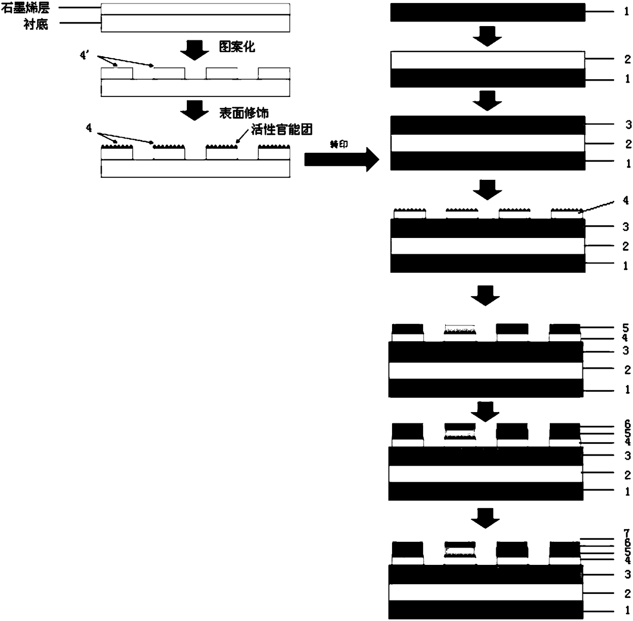
[0040] and, combined figure 1 , the embodiment of the present invention also provides a method for preparing a positive QLED device, comprising the following steps:
[0041] S01. Depositing a graphene layer on the substrate, patterning the graphene layer to form a graphene pixel array 4', modifying the surface of the graphene pixel array 4' away from the substrate, to obtain Functionalized graphene pixel array4;
[0042] S02. Provide an anode 1, deposit a hole injection layer 2 and a hole transport layer 3 sequentially on the anode 1, then transfer the functionalized graphene pixel array 4 onto the hole transport layer 3, and make the modification The treated surface faces away from said hole transport layer 3;
[0043] S03. On the functionalized graphene pixel array 4, deposit the quantum dot light-emitting layer 5, the electron transport layer 6 and the cathode 7 in sequence.
[0044] Specifically, in the above step S01 , the method for depositing the graphene layer on th...
Embodiment 1
[0059] A method for preparing a positive-type printed quantum dot light-emitting diode, comprising the following steps:
[0060] S11. Adopting CVD method to prepare a graphene layer with a thickness of 20nm on the copper sheet, transfer the graphene layer to the silicon chip, and etch the graphene layer into graphene with regular arrangement by photolithography For the pixel array, the graphene on the surface of the graphene pixel array is activated by concentrated sulfuric acid, so that the surface has a large number of active functional groups to obtain a functionalized graphene pixel array;
[0061] S12. Print the PEDOT hole injection layer and the TFB hole transport layer sequentially on the ITO anode, and then transfer the functionalized graphene pixel array to the TFB hole transport layer by a transfer printing method, and the functionalized graphene pixel array The surface with a large number of reactive functional groups faces away from the hole transport layer;
[00...
Embodiment 2
[0064] A method for preparing a reverse printed quantum dot light-emitting diode, comprising the following steps:
[0065] S21. Adopting CVD method to prepare a graphene layer with a thickness of 20nm on the copper sheet, transfer the graphene layer to the silicon chip, and etch the graphene layer into graphene with regular arrangement by photolithography For the pixel array, the graphene on the surface of the graphene pixel array is activated by concentrated sulfuric acid, so that the surface has a large number of active functional groups to obtain a functionalized graphene pixel array;
[0066] S22. Print the ZnO electron transport layer sequentially on the Al cathode, and then transfer the functionalized graphene pixel array to the ZnO electron transport layer by a transfer printing method, and the functionalized graphene pixel array has a surface with a large number of active functional groups on the back For the ZnO electron transport layer;
[0067] S23. Using a printin...
PUM
| Property | Measurement | Unit |
|---|---|---|
| Thickness | aaaaa | aaaaa |
| Thickness | aaaaa | aaaaa |
Abstract
Description
Claims
Application Information
 - R&D
- Intellectual Property
- Life Sciences
- Materials
- Tech Scout
- Unparalleled Data Quality
- Higher Quality Content
- 60% Fewer Hallucinations
Browse by: Latest US Patents, China's latest patents, Technical Efficacy Thesaurus, Application Domain, Technology Topic, Popular Technical Reports.
© 2025 PatSnap. All rights reserved.Legal|Privacy policy|Modern Slavery Act Transparency Statement|Sitemap|About US| Contact US: help@patsnap.com