High-efficient undoped ultrathin light-emitting layer thermal activation delay fluorescent organic light-emitting diode and preparation method thereof

A thermal activation delay, light-emitting diode technology, applied in semiconductor/solid-state device manufacturing, electrical components, electrical solid-state devices, etc., can solve the problems of material difficulties, increased device manufacturing process difficulties, and device manufacturing process difficulties. Quenching effect, significant external quantum efficiency, and the effect of reducing the difficulty of device fabrication

Active Publication Date: 2019-01-18
SOUTH CHINA UNIV OF TECH
View PDF3 Cites 7 Cited by
  • Summary
  • Abstract
  • Description
  • Claims
  • Application Information

AI Technical Summary

Problems solved by technology

[0003] However, both phosphorescent materials and TADF materials have serious concentration quenching effects, and it is difficult to achieve high-efficiency light emission on the basis of non-doped device structures, and it is also very difficult to develop new high-efficiency non-doped TADF materials. The current strategy Both uniformly disperse the guest luminescent material in the host material to suppress the aggregation and quenching of guest molecules.
Although this method of host-guest doping system can suppress the concentration quenching effect and improve the performance of the device, it is necessary to precisely control the evaporation rate of the host and guest materials in the preparation process of the evaporation-type device, resulting in the The difficulty of the preparation process has been greatly improved
If the currently widely commercialized co-host strategy (two host materials) is adopted, then ternary doping technology is required, and the difficulty of the device fabrication process will further increase

Method used


Image

  • High-efficient undoped ultrathin light-emitting layer thermal activation delay fluorescent organic light-emitting diode and preparation method thereof
  • High-efficient undoped ultrathin light-emitting layer thermal activation delay fluorescent organic light-emitting diode and preparation method thereof
  • High-efficient undoped ultrathin light-emitting layer thermal activation delay fluorescent organic light-emitting diode and preparation method thereof

Examples


Embodiment 1

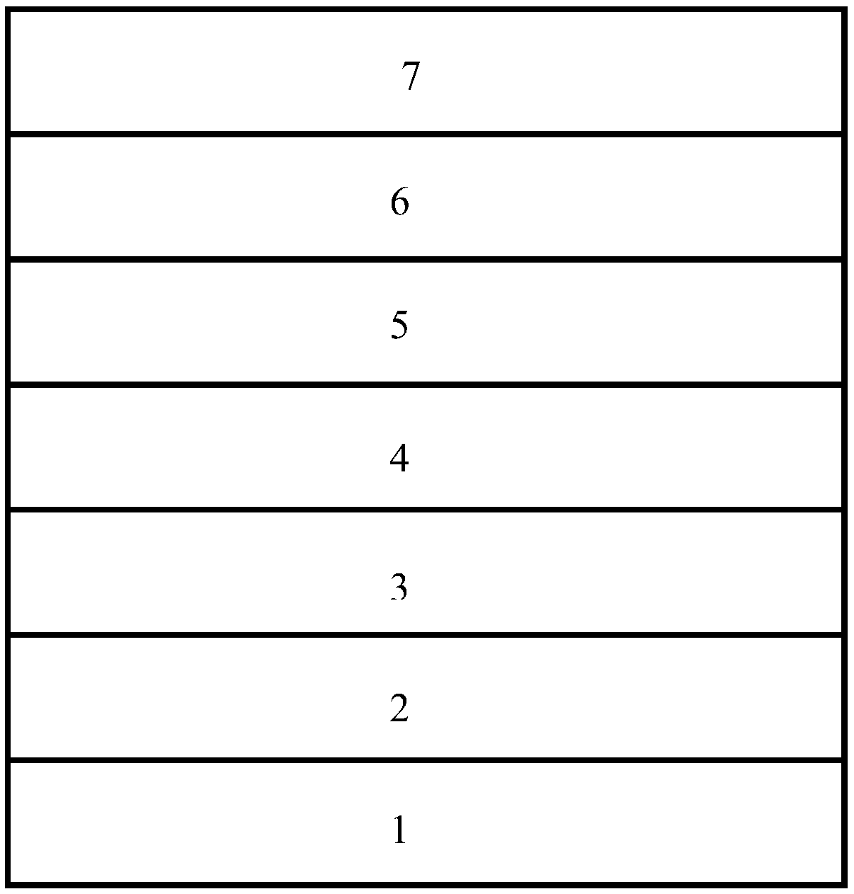
[0046] like figure 1 As shown, the high-efficiency non-doped ultra-thin light-emitting layer thermally activated delayed fluorescence organic light-emitting diode of this embodiment is composed of substrate 1, anode 2, hole transport layer 3, exciton isolation layer 4, light-emitting layer 5, Electron transport layer 6 and cathode 7 constitute.

[0047] Take a 15-20Ωsq covered with a 95nm thick sheet resistor -1 Indium tin oxide (ITO) glass substrate. First, thoroughly clean the substrate, and ultrasonically clean it in isopropanol, tetrahydrofuran, micron-sized conductive glass washing liquid, deionized water (resistivity greater than 18MΩ), deionized water, and isopropanol in an ultrasonic machine. Steps Sonicate for at least 10 minutes. Then dry it thoroughly in an electric blast drying oven to remove residual solvent on the surface. Then ionized oxygen treatment was carried out for 20 minutes to remove the pollutants on the ITO surface, improve the work function of the...

Embodiment 2

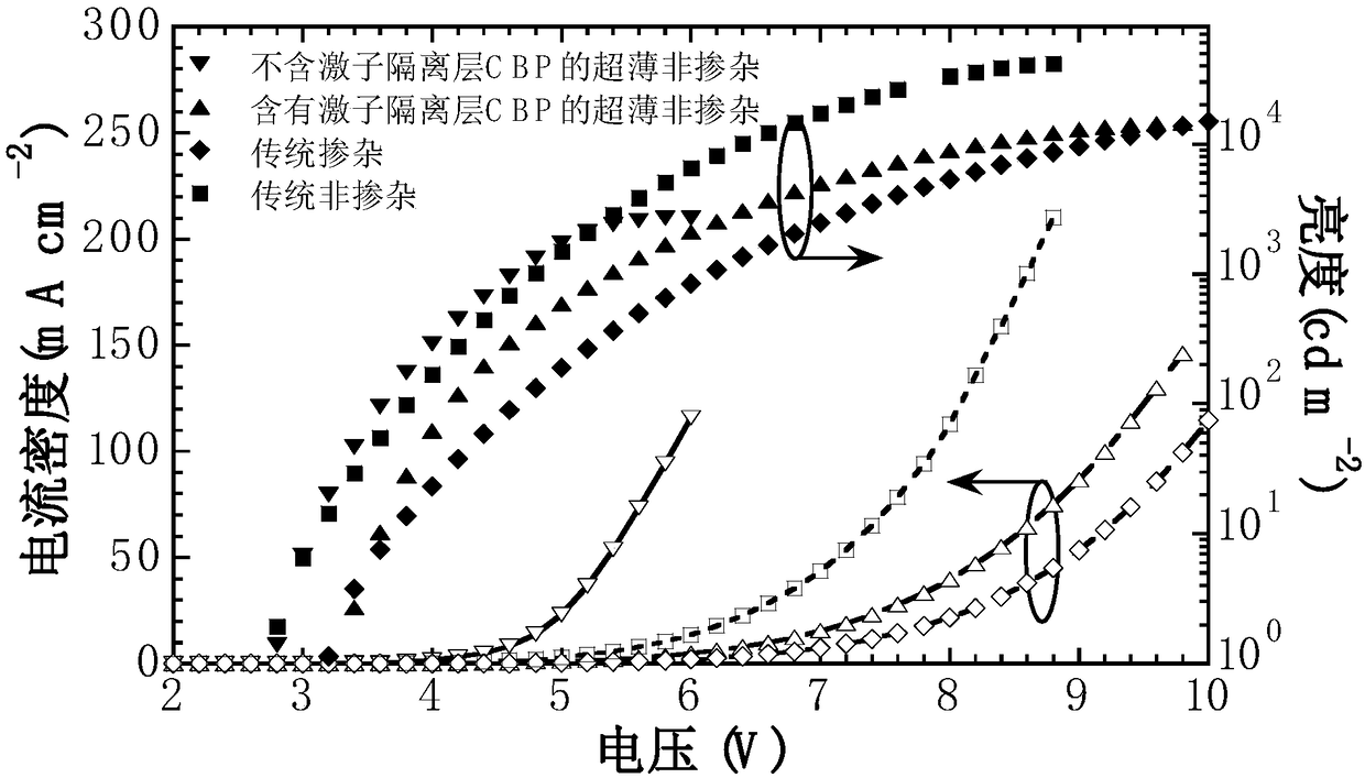
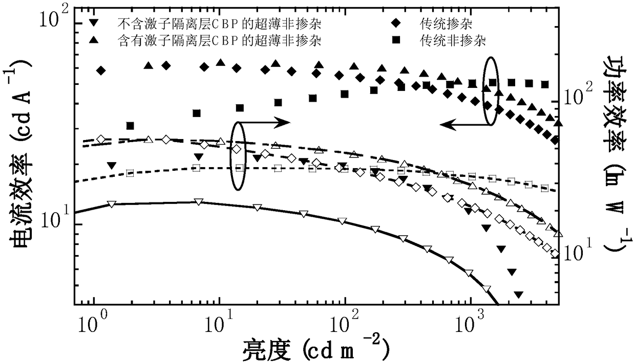
[0056] The preparation process was the same as in Example 1, wherein the non-doped ultra-thin light-emitting layer material was replaced by p-ACR-SO, and the thicknesses were 0.08, 0.1, 0.2, 0.4, 0.8, 1.2 nm. The obtained device structure is: ITO(95nm) / TAPC(30nm) / CBP(25nm) / p-ACR-SO(0.08, 0.1, 0.2, 0.4, 0.8, 1.2nm) / TmPyTB(55nm) / LiF(1nm) / Al (100nm). The corresponding conventional doped and undoped device structures are: ITO (95nm) / TAPC (30nm) / CBP:10%p-ACR-SO (25nm) / TmPyTB (55nm) / LiF (1nm) / Al (100nm ); ITO(95nm) / TAPC(30nm) / p-ACR-SO(25nm) / TmPyTB(55nm) / LiF(1nm) / Al(100nm).

[0057] The current density-brightness-voltage characteristic curve, current efficiency-brightness-power characteristic curve efficiency diagram, and external quantum efficiency-brightness characteristic curve diagram of the above-mentioned three types of devices obtained in this embodiment are shown in Figure 7-9 shown.

[0058] Table 2 is a summary table of performance data of devices with different non-do...

Embodiment 3

[0062] The preparation process was the same as in Example 1, wherein the material of the non-doped ultra-thin light-emitting layer was replaced by TZ-SBA, and the thicknesses were 0.2, 0.3, 0.4, 0.5, 0.6, 0.7, 0.8 nm. The exciton isolation layer was replaced by DEEPO with a thickness of 2nm. A hole blocking layer mCP and an electron blocking layer DPEPO are simultaneously introduced. The resulting device structure is: ITO(95nm) / TAPC(30nm) / mCP(10nm) / DPEPO(2nm) / TZ-SBA(0.2, 0.3, 0.4, 0.5, 0.6, 0.7, 0.8nm) / DPEPO(10nm) / TmPyTB(40nm) / LiF(1nm) / Al(100nm). The corresponding traditional doped and undoped device structures are: ITO (95nm) / TAPC (30nm) / mCP (10nm) / DPEPO:20% TZ-SBA (30nm) / DPEPO (10nm) / TmPyTB (40nm) / LiF(1nm) / Al(100nm); ITO(95nm) / TAPC(30nm) / mCP(10nm) / TZ-SBA(30nm) / DPEPO(10nm) / TmPyTB(40nm) / LiF(1nm) / Al(100nm ). In addition, in order to ensure that the overall thickness of the comparison device is consistent, the doped and non-doped device structures with the same thickness a...


PUM


Abstract

The invention discloses an efficient undoped ultra-thin luminescent layer thermal activation delay fluorescence organic light emitting diode, which is composed of a substrate, an anode, a hole transport layer, an exciton isolation layer, an ultra-thin thermal activation delay fluorescence light emitting layer, an electron transport layer and a cathode which are stacked in sequence. The invention also discloses a preparation method of the organic light emitting diode. An exciton isolation layer is introduced into the present invention, The exciton quenching effect of the spatially separated exciton formed by the hole transport material and the electron transport material is suppressed. Meanwhile, the dispersion degree of the thermally activated retarded fluorescent luminescent material is adjusted by using the ultra-thin undoped luminescent layer to control the thickness of the ultra-thin luminescent layer, and the concentration quenching effect of the ultra-thin undoped luminescent layer is suppressed. The invention greatly improves the performance of the undoped thermal activation delay fluorescent organic light emitting diode, reduces the preparation process difficulty of the device, saves the production time, greatly saves the use amount of the luminescent material, and has a wide application prospect.

Description

technical field [0001] The invention relates to the field of organic electroluminescent devices, in particular to a heat-activated delayed fluorescent organic light-emitting diode with a high-efficiency non-doped ultra-thin light-emitting layer and a preparation method thereof. Background technique [0002] Currently, organic light-emitting diodes (OLEDs) have been applied in the fields of light emission and display. The luminescent materials used therein can be roughly divided into three categories: traditional fluorescent materials, phosphorescent materials, and thermally activated delayed fluorescence (TADF) materials. Since the theoretical limit of internal quantum efficiency of traditional fluorescent materials is only 25%, while phosphorescent materials and TADF materials can achieve 100% internal quantum efficiency, it is of great significance to develop highly efficient phosphorescent and TADF materials. Among them, phosphorescent materials contain precious rare met...

Claims


Application Information

Patent Timeline
Patent Type & Authority Applications(China)
IPC IPC(8): H01L51/50H01L51/54H01L51/56
CPCH10K71/164H10K85/633H10K85/615H10K85/631H10K85/654H10K85/6576H10K85/6572H10K50/125H10K71/00
Inventor 苏仕健高阔徐志达
Owner SOUTH CHINA UNIV OF TECH
Why Eureka
Try Eureka