Method for detecting voids in dielectric layer and method for manufacturing semiconductor device

A dielectric layer, void detection technology, applied in semiconductor/solid-state device manufacturing, semiconductor/solid-state device testing/measurement, electrical components, etc., can solve the problems of increased R&D costs, limited number of samples, small gaps, etc., to save cost, improved deposition performance, avoided effects of time

Active Publication Date: 2021-01-01
WUHAN XINXIN SEMICON MFG CO LTD
View PDF8 Cites 0 Cited by
  • Summary
  • Abstract
  • Description
  • Claims
  • Application Information

AI Technical Summary

Problems solved by technology

[0003] 1. The structural design of the chip: There are usually many MOS field effect transistor structures formed in the dielectric layer of the chip, and generally conductive contact plugs need to be formed on the gate, source and drain of each MOS field effect transistor. However, the gap between the gate and the gate is small, and it is easier to form a void in the gate gap when depositing the dielectric
Therefore, the design of the gap between the gates and the slope angle of the gate sidewall in the structure of the chip may cause voids in the deposited dielectric layer
[0004] 2. The design problem of CVD process: For example, when the deposition speed of the dielectric material set on the CVD machine is too fast, it may cause the dielectric material to be quickly stacked in the gap between the gate and the gate, so that the stacked dielectric material Formation of voids between the electrode and the underlying deposited dielectric
If the chip is in the research and development stage, this process greatly increases the development time of the chip, affects the development progress of new products, and leads to an increase in research and development costs; if the chip has been mass-produced, a large number of abnormal chips containing holes may be produced during this period, thus Leading to a decline in the yield rate of the chip and a serious loss of production costs
In addition, FA analysis uses a limited number of samples, the process is complex, and it is difficult to quantify the exact location and number of conductive contact plug bridging defects (i.e., voids in the dielectric layer)

Method used


Image

  • Method for detecting voids in dielectric layer and method for manufacturing semiconductor device
  • Method for detecting voids in dielectric layer and method for manufacturing semiconductor device
  • Method for detecting voids in dielectric layer and method for manufacturing semiconductor device

Examples


Embodiment Construction

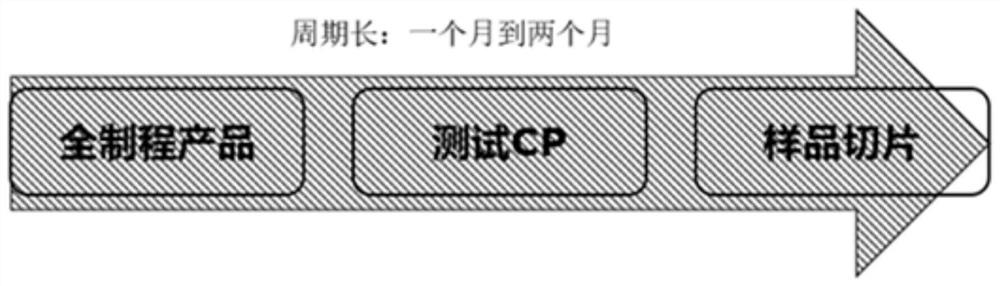
[0048] As mentioned in the background technology, in the prior art, for the detection of voids in the dielectric layer, it is necessary to perform CP test on the full-process product after obtaining the full-process product, and then further perform sample slicing for failure analysis, such as Figure 1b As shown, this method has a long cycle, high cost, and is difficult to quantify.

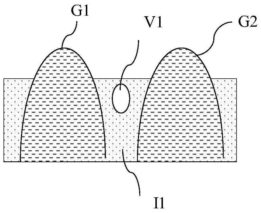
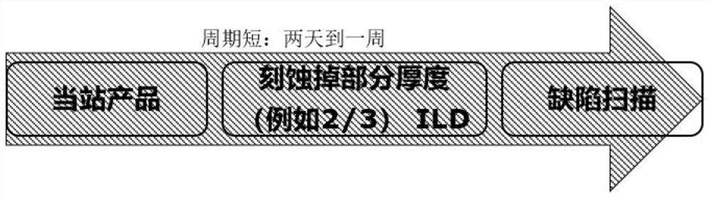
[0049] Based on this, the present invention provides a method for detecting voids in dielectric layers, please refer to Figure 2a , the detection of voids in the dielectric layer is carried out at the local station, that is, after the current station product is obtained, the dielectric layer of the current station product is first etched and thinned, exposing the corresponding part of the conductive contact plug. According to the stronger optical signal of the conductive contact plug, the position where the side wall of the conductive contact plug is bridged is easier to be found by the defect ...


PUM


Abstract

The present invention provides a method for detecting voids in a dielectric layer and a method for manufacturing a semiconductor device. The method for detecting voids in a dielectric layer includes: firstly, providing a substrate with a dielectric layer, the A plurality of conductive contact plugs are formed in the dielectric layer; then, part of the thickness of the dielectric layer is removed to expose the sidewalls of the height of the conductive contact plugs; finally, scanning has all exposed The surface of the substrate of the side wall of the conductive contact plug, to detect whether there is a bridging defect between the side walls of the adjacent conductive contact plug, the position of the bridging defect is the dielectric layer The location where voids are created during deposition. The technical solution of the present invention can quickly and accurately detect the position and quantity of bridging defects in the dielectric layer, so as to obtain the position and quantity of voids in the dielectric layer, thereby accelerating the research and development progress of semiconductor devices And improve the yield rate of semiconductor devices, and ultimately save costs.

Description

technical field [0001] The invention relates to the field of integrated circuit manufacturing, in particular to a method for detecting voids in a dielectric layer and a method for manufacturing semiconductor devices. Background technique [0002] In the structure of the chip, the conductive contact plug (CT) in the dielectric layer (ILD) plays a key connection role, and the performance of the conductive contact plug is a key factor affecting the performance of the chip. However, in the actual manufacturing of chips, during the process of depositing the dielectric layer, voids (Void) may be generated in the dielectric layer, and multiple contacts for filling the conductive contact plugs are formed when the dielectric layer is etched. When the holes are formed, the voids generated may cause two or more adjacent contact holes to be connected. When these contact holes are filled with metals such as tungsten, the metal will also fill the voids in the dielectric layer connected to...

Claims


Application Information

Patent Timeline
Patent Type & Authority Patents(China)
IPC IPC(8): H01L21/66H01L21/02
CPCH01L21/02107H01L22/12
Inventor 贾洋周伦潮冯巍奉伟
Owner WUHAN XINXIN SEMICON MFG CO LTD
Why Eureka
Try Eureka