Titanium dioxide film gas sensor with niobium-doped anatase phase and manufacturing method for same
A gas sensor, titanium dioxide technology, applied in the sensor field, can solve the problems of wide detection range, low detection limit, complex process, etc., and achieve the effect of wide detection range, low detection limit, and improved sensitivity
- Summary
- Abstract
- Description
- Claims
- Application Information
AI Technical Summary
Problems solved by technology
Method used
Image
Examples
preparation example Construction
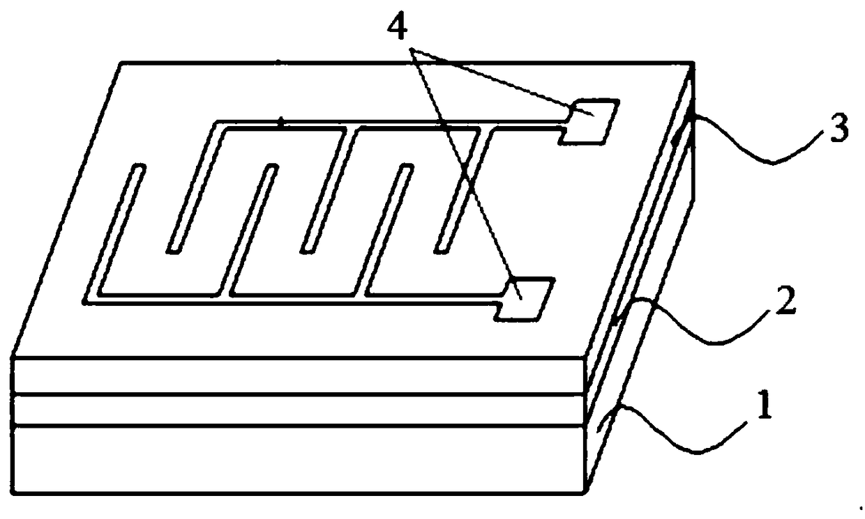
[0032] A method for preparing a niobium-doped anatase phase titanium dioxide film gas sensor, comprising the following steps:
[0033] (1) Sputtering a niobium-doped titanium dioxide seed layer on the substrate surface; the sputtering target is Nb x Ti 2-x o 3 , where x=0.05~0.2;
[0034] (2) performing the first annealing on the substrate sputtered with the niobium-doped titanium dioxide seed layer in the step (1), forming a niobium-doped anatase phase titanium dioxide seed layer on the substrate surface;
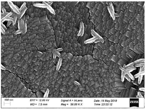
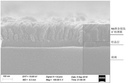
[0035] (3) The seed layer of the substrate obtained in the step (2) with the niobium-doped anatase phase titanium dioxide seed layer on the surface is immersed downward in the hydrothermal reaction precursor solution, and the hydrothermal reaction is carried out on the substrate A niobium-doped anatase titanium dioxide film is formed on the bottom surface; the hydrothermal reaction precursor solution includes water, hydrochloric acid, a titanium dioxide precursor and ni...
Embodiment 1
[0052] (1) Use acetone, ethanol, and deionized water in sequence to ultrasonically clean the glass substrate, and dry it in a drying oven;
[0053] (2) Magnetron sputtering niobium-doped titanium dioxide seed layer: the Nb 0.12 Ti 1.88 O 3 The target is installed on the cathode target position of the magnetron sputtering system, the distance between the target and the substrate is adjusted to 60mm, and the Nb 0.12 Ti 1.88 O 3 The RF sputtering power of the target is 60w, and the sputtering deposition is continued on the cleaned and dried glass substrate for 40min to form a niobium-doped titanium dioxide seed layer on the surface of the substrate;
[0054] (3) Anneal the sample obtained in step 2 at 400 °C for 1 h under high vacuum to obtain a niobium-doped anatase phase titanium dioxide seed layer, and the annealing vacuum degree is less than 10 -3 Pa;
[0055] (4) carry out hydrothermal reaction:
[0056] Configure the hydrothermal reaction precursor solution: water, e...
Embodiment 2
[0078] Other conditions were the same as in Example 1, except that the hydrothermal reaction temperature in step (4) was changed to 120°C, and the hydrothermal reaction time was changed to 5h.
PUM
| Property | Measurement | Unit |
|---|---|---|
| thickness | aaaaa | aaaaa |
| thickness | aaaaa | aaaaa |
| thickness | aaaaa | aaaaa |
Abstract
Description
Claims
Application Information


