A photosensitive sensor based on an organic field effect tube and its preparation method

A photosensitive sensor and organic field technology, applied in the sensor field, can solve the problems of poor stability and low responsivity of the photosensitive sensor, and achieve the effects of rich content, high responsivity and simple extraction process

Active Publication Date: 2020-06-23
UNIV OF ELECTRONICS SCI & TECH OF CHINA
View PDF5 Cites 0 Cited by
  • Summary
  • Abstract
  • Description
  • Claims
  • Application Information

AI Technical Summary

Problems solved by technology

[0005] The object of the present invention is to: aim at the problem of poor stability and low responsivity of traditional field effect tube photosensitive sensors, provide a kind of photosensitive sensor based on organic field effect tube and its preparation method, adopt biological material to prepare photosensitive sensor, not only process is simple, The production cost is low, and the photosensitive sensor has high responsivity, high stability and long life

Method used


Image

  • A photosensitive sensor based on an organic field effect tube and its preparation method
  • A photosensitive sensor based on an organic field effect tube and its preparation method
  • A photosensitive sensor based on an organic field effect tube and its preparation method

Examples


preparation example Construction

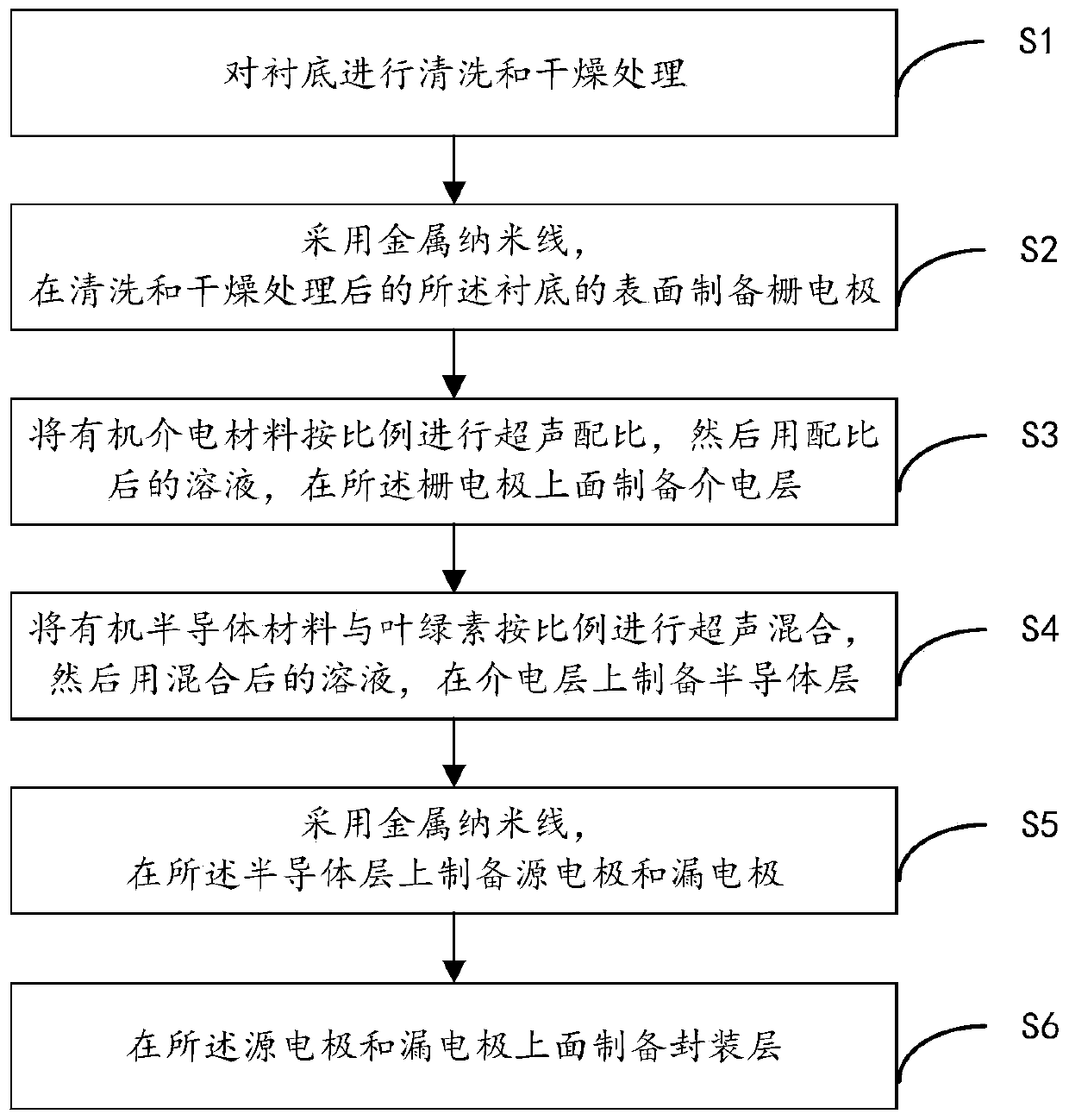
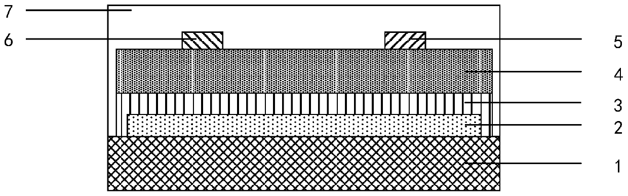
[0041] A method for preparing a photosensitive sensor based on an organic field effect transistor, such as figure 1 shown, including the following steps:

[0042] S1, cleaning and drying the substrate 1;

[0043] S2. Using metal nanowires, prepare a gate electrode 2 on the surface of the substrate 1 after cleaning and drying;

[0044] S3, ultrasonically proportioning the organic dielectric material in proportion, and then using the proportioned solution to prepare a dielectric layer 3 on the gate electrode 2;

[0045] S4, ultrasonically mixing the organic semiconductor material and chlorophyll in proportion, and then using the mixed solution to prepare a semiconductor layer 4 on the dielectric layer 3;

[0046] S5. Prepare a source electrode 5 and a drain electrode 6 on the semiconductor layer 4 by using metal nanowires;

[0047] S6 , preparing an encapsulation layer 7 on the source electrode 5 and the drain electrode 6 .

[0048] Further, the dielectric layer 3 in step S3 a...

Embodiment 1

[0059] A method for preparing a photosensitive sensor based on an organic field effect tube provided in this embodiment includes:

[0060] Step 1. Clean the substrate 1 with detergent, acetone solution, deionized water and isopropanol solution, and dry it with nitrogen after cleaning;

[0061] Step 2, using silver nanowires, through a method in vacuum thermal evaporation, magnetron sputtering, plasma enhanced chemical vapor deposition, screen printing, printing or spin coating, after cleaning and drying, the preparing a gate electrode 2 on the surface of the substrate 1;

[0062] Step 3. Ultrasonic proportioning of polystyrene (PS) according to a certain concentration, and then using the proportioned solution, through one of the methods of spin coating, roller coating, drop film, embossing, printing or spraying, in the place A dielectric layer 3 with a thickness of 500 nm is prepared on the gate electrode 2;

[0063] Step 4, ultrasonically mix 3-hexylthiophene (P3HT) and chl...

Embodiment 2

[0067] A method for preparing a photosensitive sensor based on an organic field effect tube provided in this embodiment includes:

[0068] Step 1. Clean the substrate 1 with detergent, acetone solution, deionized water and isopropanol solution, and dry it with nitrogen after cleaning;

[0069] Step 2, using gold nanowires, through a method in vacuum thermal evaporation, magnetron sputtering, plasma enhanced chemical vapor deposition, screen printing, printing or spin coating, after cleaning and drying, the preparing a gate electrode 2 on the surface of the substrate 1;

[0070] Step 3, ultrasonically proportioning polymethyl methacrylate according to a certain concentration, and then using the proportioned solution, through one of the methods of spin coating, roller coating, drop film, embossing, printing or spraying, in the place A dielectric layer 3 with a thickness of 300 nm is prepared on the gate electrode 2;

[0071] Step 4. Ultrasonic mixing Tips-pentacene (Tips-penta...


PUM

PropertyMeasurementUnit
thicknessaaaaaaaaaa
thicknessaaaaaaaaaa
thicknessaaaaaaaaaa

Abstract

The invention discloses a photosensitive sensor based on an organic field effect transistor and a preparation method thereof. The preparation method includes: cleaning and drying a substrate; using metal nanowires, after cleaning and drying the substrate The gate electrode is prepared on the surface of the gate electrode; the organic dielectric material is ultrasonically proportioned in proportion, and then a dielectric layer is prepared on the gate electrode with the proportioned solution; the organic semiconductor material and chlorophyll are ultrasonically mixed in proportion, and then Using the mixed solution, a semiconductor layer is prepared on the dielectric layer; metal nanowires are used to prepare source and drain electrodes on the semiconductor layer; and shellac is used to prepare an encapsulation layer on the source and drain electrodes. The invention prepares the semiconductor layer of the photosensitive sensor by using the mixed material of organic semiconductor material and chlorophyll, so that the prepared photosensitive sensor has the characteristics of high responsivity and high stability compared with the traditional photosensitive sensor.

Description

technical field [0001] The invention belongs to the technical field of sensors, in particular to a photosensitive sensor based on an organic field effect tube and a preparation method thereof. Background technique [0002] The application fields of sensors are very broad. It can be said that from space to the ocean, from various complex engineering systems to people's daily necessities of life, all kinds of sensors are inseparable. Sensing technology plays an increasingly important role in the development of the national economy. Huge effect. Compared with traditional photoresistive devices, organic field-effect transistor photosensors have the advantages of high responsivity, room temperature operation, easy integration, and independent multi-parameters to improve selectivity. , Inexpensive, flexible, simple preparation method, many types, performance can be adjusted by molecular design and other advantages, it has always attracted people's attention in the field of photos...

Claims


Application Information

Patent Timeline
Patent Type & Authority Patents(China)
IPC IPC(8): H01L51/46H01L51/42H01L51/48
CPCH10K71/12H10K85/30H10K30/65Y02E10/549
Inventor 于军胜邵炳尧庄昕明侯思辉
Owner UNIV OF ELECTRONICS SCI & TECH OF CHINA
Why Eureka
Try Eureka