Avalanche photodetector based on arc diffusion region and manufacturing method of avalanche photodetector

A technology of avalanche photoelectricity and diffusion area, which is applied in the direction of circuits, electrical components, semiconductor devices, etc., can solve the problems of reduced detection efficiency of single-photon detectors, decreased overall performance of devices, and low single-photon detection efficiency, so as to improve photon detection efficiency , reduce the chance of afterpulse, and gain a strong effect

Active Publication Date: 2019-02-15
INST OF SEMICONDUCTORS - CHINESE ACAD OF SCI +1
View PDF3 Cites 7 Cited by
  • Summary
  • Abstract
  • Description
  • Claims
  • Application Information

AI Technical Summary

Problems solved by technology

This inconsistency due to illumination and the spatial region where the avalanche occurs can lead to a decrease in the detection efficiency of single-photon detectors near the avalanche voltage, especially as the diameter of the device increases beyond 30 μm.
When the bias voltage is increased by a few volts, the electric field in the gain region gradually becomes uniform. At this time, the detection efficiency of the device increases slightly, but the dark count increases sharply, and the overall performance of the device decreases.
Therefore, it is urgent to propose a solution to solve the problem of low single-photon detection efficiency and high dark count caused by the misalignment between the light incident center and the avalanche multiplication area.

Method used


Image

  • Avalanche photodetector based on arc diffusion region and manufacturing method of avalanche photodetector
  • Avalanche photodetector based on arc diffusion region and manufacturing method of avalanche photodetector
  • Avalanche photodetector based on arc diffusion region and manufacturing method of avalanche photodetector

Examples


Embodiment Construction

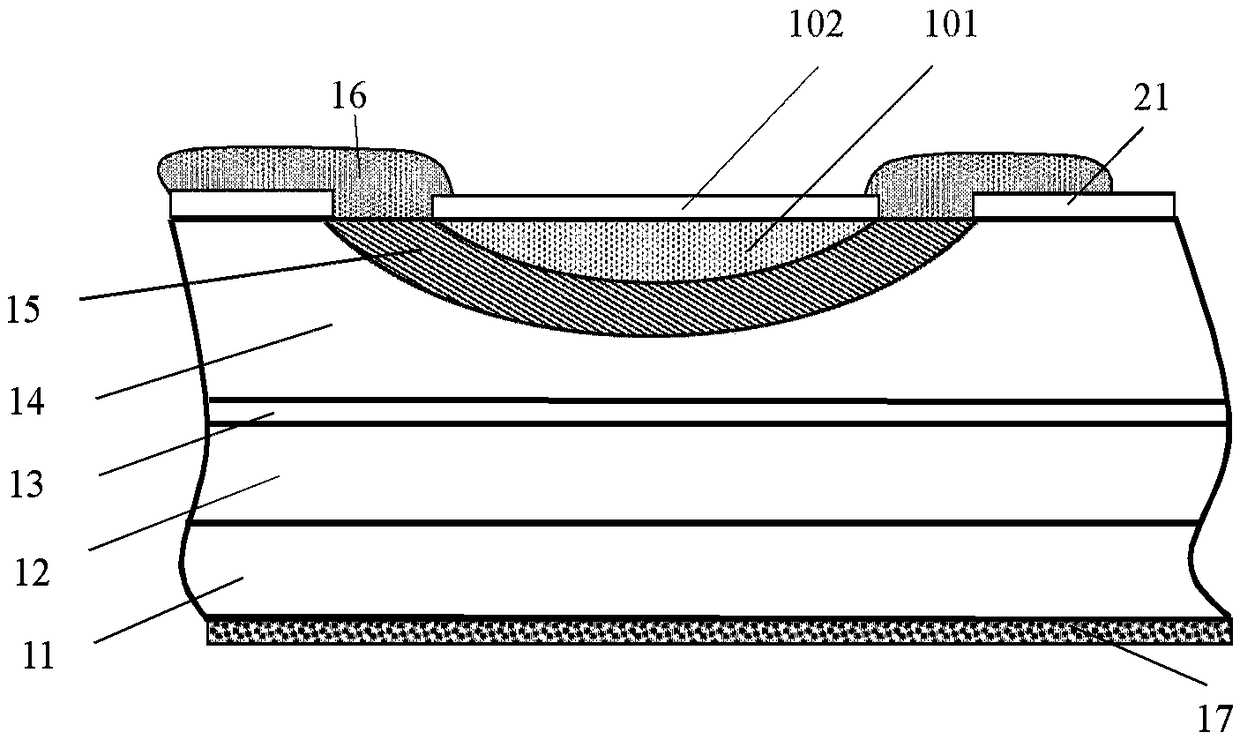
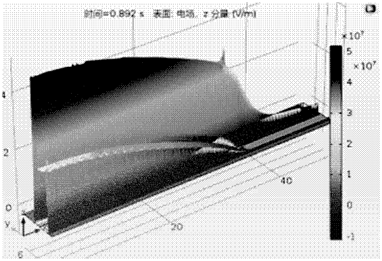
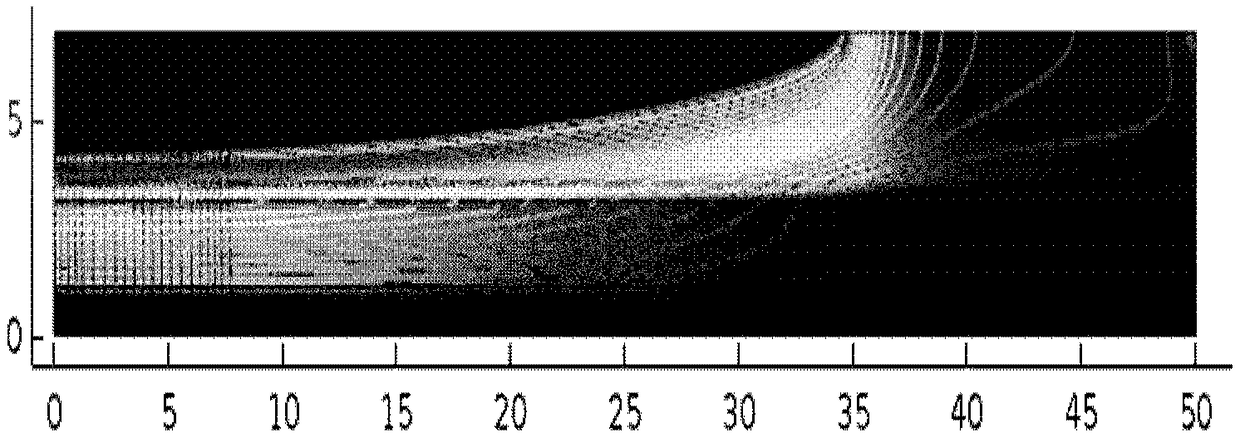
[0032] The disclosure provides an avalanche photodetector based on an arc-shaped diffusion region and its manufacturing method. By forming a 3D bowl-shaped opening in the intrinsic multiplication layer and performing high P-type doping in the bowl-shaped opening, the center of the window The partially undiffused multiplication layer has the smallest thickness, and the edge thickness is the largest, so as to form a P-type highly doped arc-shaped diffusion region, so that the central part of the light field in the multiplication region of the avalanche detector has the strongest gain, and the impact ionization of the multiplication region is more uniform in the lateral direction , reduce the edge electric field and the resulting edge breakdown, and ensure the spatial coincidence of the center light field and the strongest electric field of the device, which can effectively improve the photon detection efficiency of the device, reduce the dark count of the device, and reduce the po...


PUM


Abstract

The invention discloses an avalanche photodetector based on an arc diffusion region and a manufacturing method of the avalanche photodetector. The avalanche photodetector comprises an epitaxial structure, a passivation layer, a P type electrode layer, an N type electrode layer, and an antireflection film, wherein the epitaxial structure comprises an N-type substrate, an absorption layer, a chargelayer and an intrinsic multiplication layer from the bottom up; a 3D bowl-shaped opening is formed in the intrinsic multiplication layer, and a P-type highly-doped arc-shaped diffusion region is formed under the 3D bowl-shaped opening; the passivation layer formed on the epitaxial structure; the P-type electrode layer is in contact with the P-type highly-doped arc-shaped diffusion region; the N-type electrode layer is in contact with the N-type substrate; the antireflection film, which serves as a light window, is arranged on the front surface or the back surface of the single-electron avalanche photodetector; the connecting line of the center of the antireflection film and the curvature center of the arc-shaped diffusion area is parallel to the extension direction; and the light field central area of the light window coincides with a high field area in space. According to the avalanche photodetector, the photon detection efficiency of the device is effectively improved, the dark countof the device is reduced, and the probability of the post pulse is reduced.

Description

technical field [0001] The disclosure belongs to the technical field of semiconductor devices, and relates to an avalanche photodetector based on an arc-shaped diffusion region and a manufacturing method thereof. Background technique [0002] Avalanche photodetectors (APD, Avalanche Photo-Detector) have been widely used in commercial, military and scientific research, such as quantum information, biomolecular detection, lidar imaging and astronomical detection. The single-photon APD with high speed in the communication band, high detection efficiency, and low number of secrets has played an extremely important role in the actual quantum key distribution system. Single Photon Avalanche Photodetector (SPAD, Single Photon Avalanche-Detector) Due to its special Geiger working method, the avalanche process and avalanche current density have a great influence on the detection efficiency and dark count of the device. The detection efficiency of the photon is low, and the high dete...

Claims


Application Information

Patent Timeline
Patent Type & Authority Applications(China)
IPC IPC(8): H01L31/107H01L31/0352H01L31/18
CPCH01L31/035272H01L31/1075H01L31/1844Y02P70/50
Inventor 杨晓红王晖何婷婷刘凯宝
Owner INST OF SEMICONDUCTORS - CHINESE ACAD OF SCI
Why Eureka
Try Eureka