Manufacturing method of trench Schottky

A manufacturing method and trench technology, applied in semiconductor/solid-state device manufacturing, electrical components, circuits, etc., can solve problems such as difficulties in epitaxial layers, and achieve the effects of improving device performance, reducing resistance, and improving performance

Inactive Publication Date: 2019-02-26
TIANJIN HUANXIN TECH DEV
View PDF4 Cites 3 Cited by
  • Summary
  • Abstract
  • Description
  • Claims
  • Application Information

AI Technical Summary

Problems solved by technology

The disadvantage of the existing technology is that the resistivity of the N- epitaxial layer determines the leakage and conduction voltage drop of the device. After the resistivity of the epitaxial layer is determined, it is very difficult to further reduce the leakage and conduction voltage drop.

Method used


Image

  • Manufacturing method of trench Schottky
  • Manufacturing method of trench Schottky
  • Manufacturing method of trench Schottky

Examples


Embodiment 1

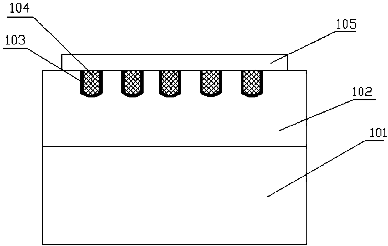
[0023] Step 1: First epitaxially layer a buffer layer on the N+ heavily doped silicon substrate, N: resistivity 0.1-20Ω.cm, thickness 1-20um, the epitaxial N of this layer mainly plays a role in ensuring the withstand voltage of the device The purpose of further reducing the forward voltage drop of the device and reducing the resistance of the drift region;

[0024] Step 2: Epitaxially layer a lightly doped layer on the buffer layer. Compared with the upper buffer layer, the doping concentration is reduced. N-: resistivity 0.3-30Ω.cm, thickness 1-20um, epitaxy N- is mainly effective Reduce the reverse leakage of the device, and optimize the withstand voltage between the barrier region and the trench by optimizing the resistivity of this layer. Both steps 1 and 2 are carried out at a temperature of 800-1150°C. The epitaxial buffer layer and the lightly doped layer are grown by the chemical vapor deposition process. The above-mentioned process is used to epitaxially buffer the l...

Embodiment 2

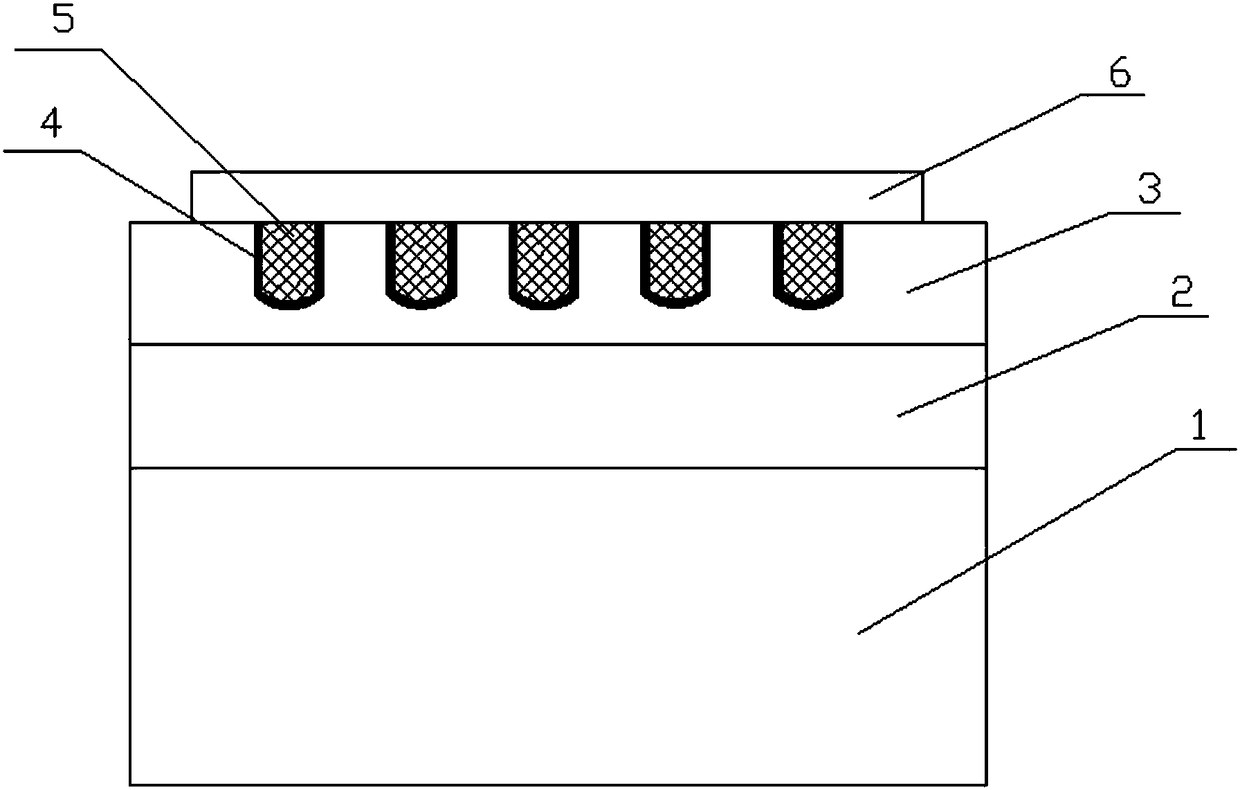
[0029] According to the different withstand voltage of the device, the number of epitaxial N-lightly doped layers in step 2 is not limited to one layer, but can be a multi-layer structure. Generally, the method of gradually reducing the doping concentration is adopted to gradually increase the resistivity of each epitaxial layer. That is, the doping concentration of each lightly doped layer gradually decreases from bottom to top, and the resistivity gradually increases accordingly. Of course, targeted optimization can also be carried out for individual layers.

[0030] Example 2 Change the epitaxial one lightly doped layer in Step 2 of Example 1 to epitaxially two lightly doped layers. The resistivity of the upper lightly doped layer is higher than that of the lower lightly doped layer, but the resistivity and thickness of each layer are still within the specified requirements. , N-: Resistivity 0.3~30Ω.cm, thickness 1~20um. Other steps are with embodiment 1.

Embodiment 3

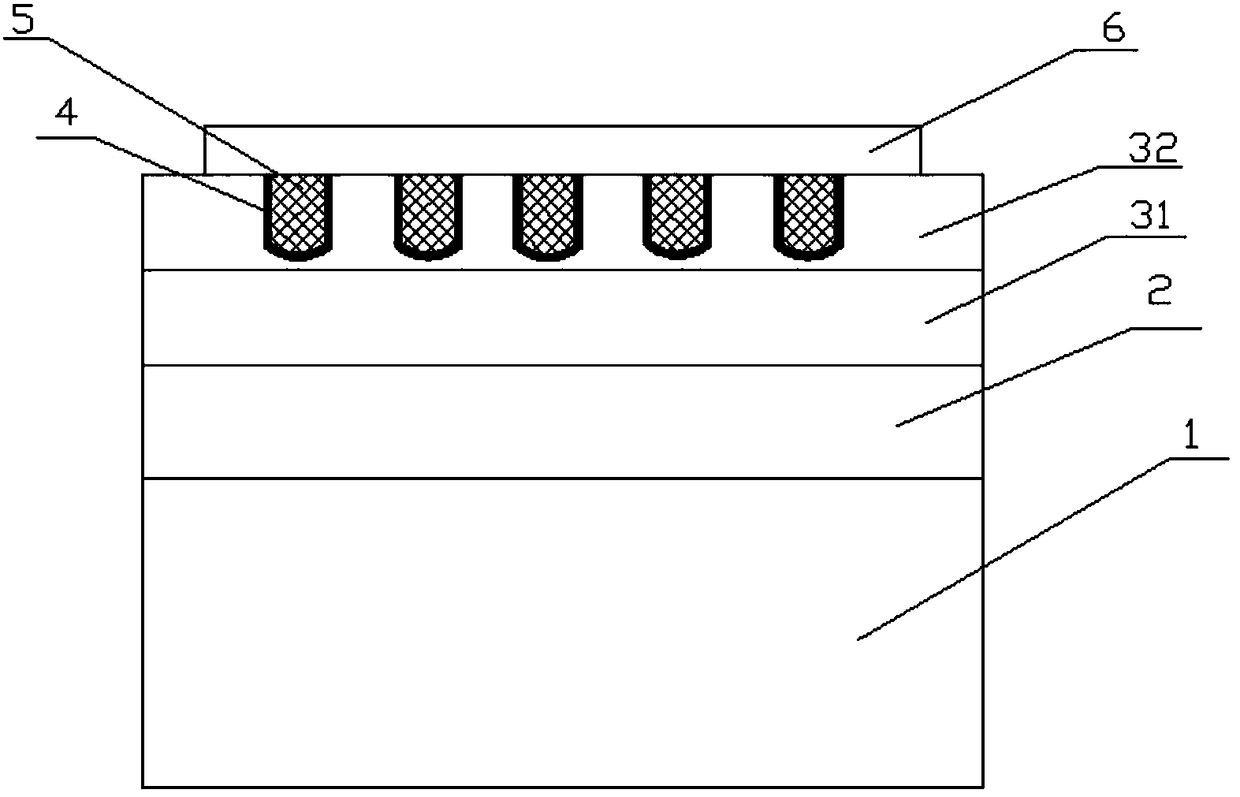
[0032] Example 3 Change the epitaxial one lightly doped layer in Step 2 of Example 1 to epitaxial four lightly doped layers. The resistivity of the four lightly doped layers gradually increases from bottom to top, but the resistivity and thickness of each layer are still specified Within the requirements, N-: resistivity 0.3~30Ω.cm, thickness 1~20um. Other steps are with embodiment 1.

[0033] In the present invention, a layer of buffer layer with a relatively higher doping concentration is first epitaxially used to further reduce the forward conduction voltage drop of the device and reduce the resistance of the drift region under the premise of ensuring the withstand voltage of the device, and then epitaxially epitaxially one or more layers The lightly doped layer with gradually reduced doping concentration makes the resistivity of each layer gradually increase, which can effectively reduce the reverse leakage of the device, realize the withstand voltage optimization between ...


PUM


Abstract

The present invention discloses a manufacturing method of trench Schottky. The method comprises the following steps of: a. performing epitaxy of a buffer layer on an N+ heavily-doped substrate; and b.growing n lightly-doped layers in order on the buffer layer. The buffer layer with relatively high dosage concentration is subjected to epitaxy and is configured to further reduce the forward conduction voltage drop of a device and reduce the resistance of a drifting region on the premise of ensuring the withstand voltage of the device, one or more than one lightly-doped layers with gradually reduced dosage concentration are subjected to epitaxy to gradually increase the electrical resistivity of each layer to effectively reduce the backward electric leakage of the device, achieve the withstand voltage optimization of a barrier region and a trench, achieve the regulation of the epitaxial electrical resistivity, effectively reduce the electric leakage and conduction voltage drop of the trench Schottky products and further improve the device performances; the substrate materials employ a multi-layer epitaxy mode to improve the performances of the device with no need for extra increasingof special processes, and compared to the complete compatibility in the prior art, the processing cost is reduced.

Description

technical field [0001] The invention relates to a Schottky manufacturing process, in particular to a trench Schottky manufacturing method. Background technique [0002] Schottky barrier diodes have been used in power supply applications for decades as rectifying devices. Compared with PN junction diodes, Schottky barrier diodes have the advantages of low forward turn-on voltage and fast switching speed, which makes them very suitable for switching power supplies and high-frequency applications. Schottky barrier diodes are manufactured using the principle of a metal-semiconductor junction formed in contact between a metal and a semiconductor. Trench Schottky adopts the principle that the trench structure produces a depletion layer to pinch off the conductive channel, and its high-frequency characteristics and electrical performance are significantly better than those of the planar Schottky. [0003] As we all know, the silicon material used in the Schottky diode chip is usu...

Claims


Application Information

Patent Timeline
Patent Type & Authority Applications(China)
IPC IPC(8): H01L21/329H01L29/872
CPCH01L29/66143H01L29/8725
Inventor 王万礼王彦君孙晨光徐长坡刘闯张晋英刘晓芳董子旭张喆张建戴明磊徐阳赵杨张飚李玉伟魏东娜马国芹张俊芳
Owner TIANJIN HUANXIN TECH DEV
Why Eureka
Try Eureka