Photoelectric coupling mechanism and manufacturing method thereof

A technology of photoelectric coupling and manufacturing method, which is applied in the coupling of optical waveguide, light guide, optics, etc., can solve the problems of inconvenient adjustment and observation of microlens array, complex and time-consuming assembly process, and small coupling tolerance, etc., and can be implemented High reliability, wide tolerance tolerance and low cost effect

Inactive Publication Date: 2019-03-01
NO 30 INST OF CHINA ELECTRONIC TECH GRP CORP
View PDF5 Cites 0 Cited by
  • Summary
  • Abstract
  • Description
  • Claims
  • Application Information

AI Technical Summary

Problems solved by technology

However, by processing a 45° optical plane on the end face of each optical fiber in the optical fiber array, using the characteristics of light cylinder gathering, it is necessary to control the angle deviation and coupling tolerance of the 45° optical plane of each optical fiber during the alignment process wi

Method used


Image

  • Photoelectric coupling mechanism and manufacturing method thereof
  • Photoelectric coupling mechanism and manufacturing method thereof
  • Photoelectric coupling mechanism and manufacturing method thereof

Examples


Example Embodiment

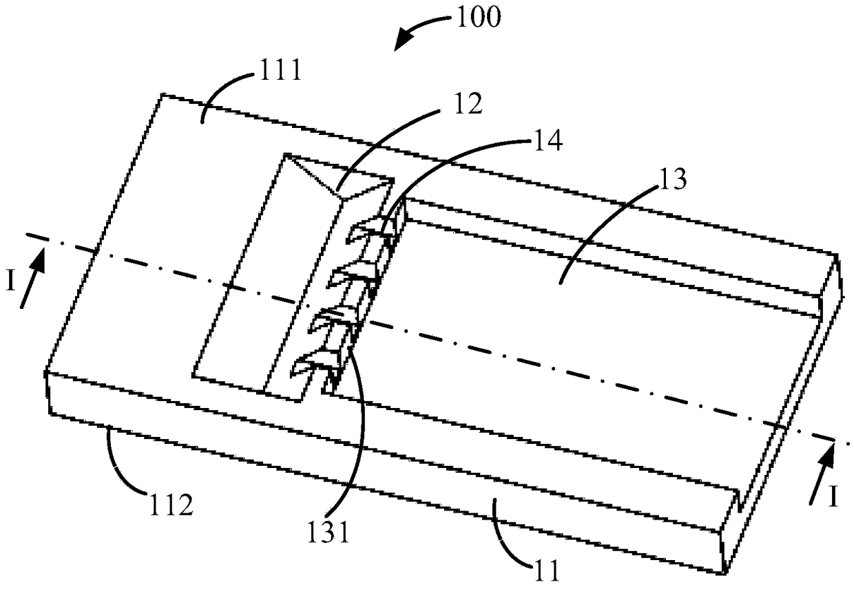
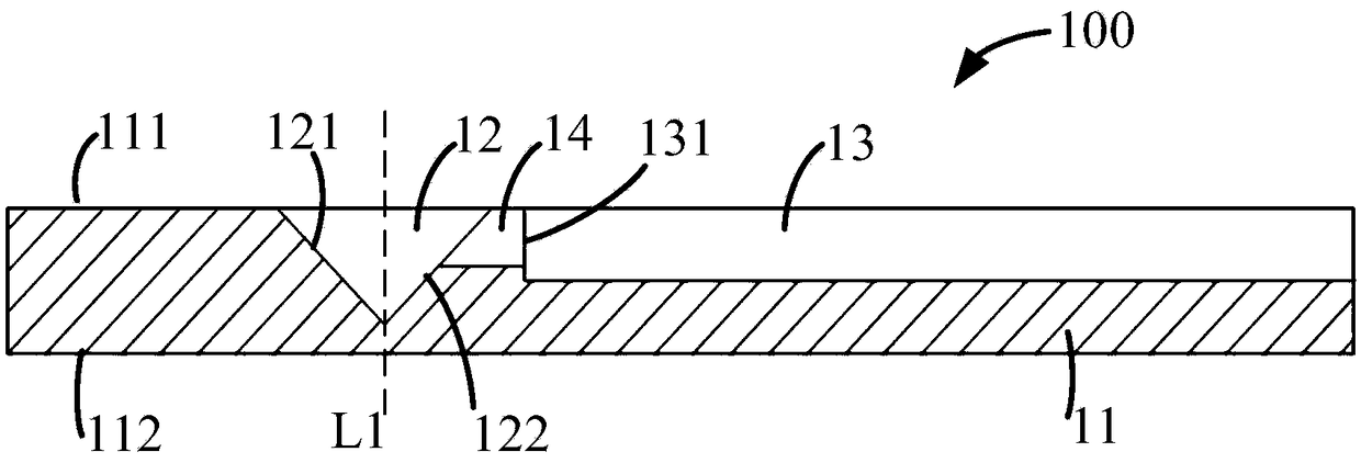
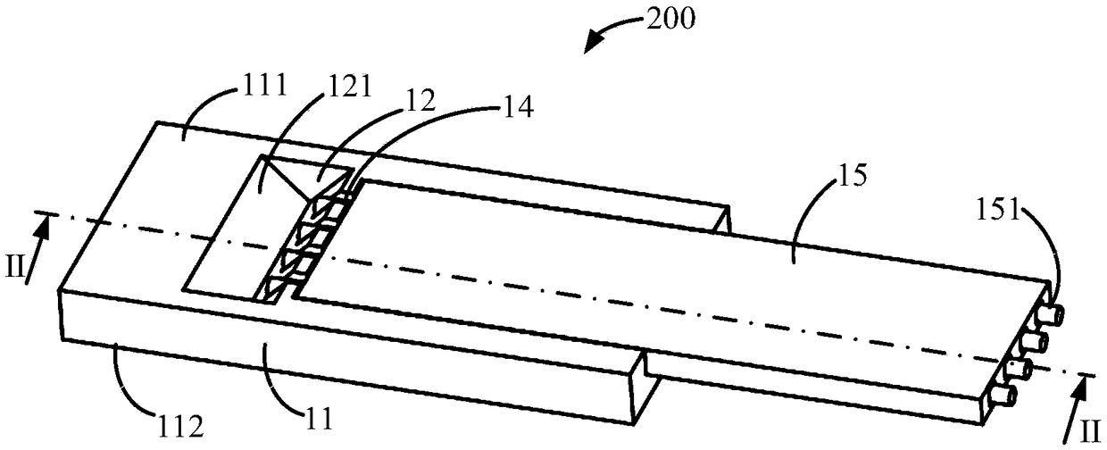
[0019] Such as Figure 1 to Figure 4 As shown, a photoelectric coupling mechanism 100 of the present invention is processed and manufactured on a rigid printed circuit board substrate 11 such as FR4 or PTFE. The substrate 11 can be a material such as FR4 or PTFE; the substrate 11 has a relatively A surface 111 and a second surface 112, and a first groove 12 and a second groove 13, both of the first groove 12 and the second groove 13 are recessed from the first surface 111 to the second surface 112; A groove 12 has a first reflective surface 121 and a second flat surface 122 perpendicular to each other, which are processed by a 90° "V" dicing machine or other methods, and the first reflective surface 121 faces the direction of the second groove 13; The included angle between the first reflecting surface 121 and the first surface 111 of the substrate 11 is 45°. Through simulation and experiment, the included angle is 43° to 47° to ensure a good coupling efficiency range; A refle...


PUM


Abstract

The invention discloses a photoelectric coupling mechanism and a manufacturing method thereof. The coupling mechanism is made of a rigid printed circuit board substrate. The substrate has a first surface, a second surface, a first trough and a second trough, wherein the first surface faces the second surface. The first trough has a first reflection surface and a second surface which are mutually perpendicular. The included angle between the first reflection surface and the substrate is 43-47 DEG. The first reflection surface is provided with a metal reflection film or a dielectric reflection film which is plated. A fiber fixing trough is arranged between the first trough and the second trough. According to the photoelectric coupling mechanism, the photoelectric coupling mechanism is manufactured on the rigid printed circuit board material, and furthermore a fiber array interconnected substrate is fixed. The photoelectric coupling mechanism is compatible with a traditional printed circuit board manufacturing process and does not require development of a new laminating process flow and equipment. The photoelectric coupling mechanism and the manufacturing method thereof have advantages of simple structure, high applicability of the manufacturing method, low cost, simple assembling process, wide tolerance, and coupling efficiency improvement between a parallel photoelectric array chip and a fiber array.

Description

technical field [0001] The invention relates to a photoelectric coupling mechanism and a manufacturing method thereof. Background technique [0002] With the rapid development of high-speed communication technology, the amount of information has grown exponentially. Humans urgently need electronic communication systems with high speed, high bandwidth, large capacity, low bit error rate, low power consumption and anti-electromagnetic interference capabilities. Traditional electrical interconnection methods cannot meet the current needs and have become a bottleneck restricting the rapid development of high-speed electronic communication systems. The photoelectric interconnection circuit using optical transmission can realize high-speed, high-bandwidth, high-density, and low-power information transmission between boards, components, and chips within the electronic communication system, and can effectively solve the transmission bottleneck of high-speed electrical interconnectio...

Claims


Application Information

Patent Timeline
IPC IPC(8): G02B6/42G02B6/43
CPCG02B6/4214G02B6/4239G02B6/4243G02B6/43
Inventor 毛久兵杨伟李建平冯晓娟杨平吴圣陶刘恒刘鹏刘平李澄宇杨剑
Owner NO 30 INST OF CHINA ELECTRONIC TECH GRP CORP
Why Eureka
Try Eureka