Groove preparation method of GaN-based material

A base material, non-concave technology, applied in the field of groove preparation of GaN base materials, can solve the problems of deterioration of GaN surface characteristics, affecting the dynamic characteristics of the device, affecting the electrical characteristics of the device, etc., which is conducive to large-scale implementation and high operability. and repeatability, the effect of improving device performance

Active Publication Date: 2019-03-01
INST OF ELECTRONICS ENG CHINA ACAD OF ENG PHYSICS
View PDF3 Cites 1 Cited by
  • Summary
  • Abstract
  • Description
  • Claims
  • Application Information

AI Technical Summary

Problems solved by technology

However, the thinning of the barrier layer of groove technology is usually done by dry etching. On the one hand, dry etching causes uneven etching depth due to the difficulty of precise control of precision, and on the other hand, the etching process causes a large number of surface defects. Seriously affect the electrical characteristics of the device
Another groove technology uses high-temperature oxidation and wet etching to achieve self-stop thinning of the barrier layer. However, due to long-term high-temperature oxidation in this process, the surface characteristics of GaN are likely to deteriorate, which seriously affects the dynamic characteristics of the device.

Method used


Image

  • Groove preparation method of GaN-based material
  • Groove preparation method of GaN-based material
  • Groove preparation method of GaN-based material

Examples


Embodiment Construction

[0028] The present invention will be described in detail below through specific embodiments and accompanying drawings.

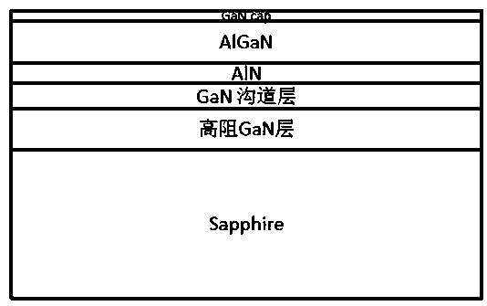
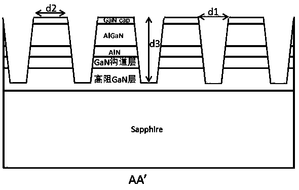
[0029] Taking AlGaN / GaN materials as an example, figure 1 It is the specific epitaxial wafer structure of this embodiment, including from bottom to top: 1) epitaxial substrate Sapphire; 2) GaN buffer; 3) sacrificial layer, namely 2nm AlN, with a thickness of 1-5nm; 4) barrier layer, That is, 20nm AlGaN; 5) GaN capping layer (GaN cap), the thickness of which is 2-5nm, and 2nm is selected for specific preparation in this embodiment.

[0030] The method of etching the non-groove area can be selected by ICP etching or RIE etching.

[0031] The depth of the etched non-groove region is greater than the sum of the thicknesses of the sacrificial layer, the barrier layer and the GaN capping layer, that is, it needs to be etched at least to the GaN buffer layer.

[0032] Further, the corrosive solution can selectively corrode only the sacrificial layer without affec...


PUM

PropertyMeasurementUnit
thicknessaaaaaaaaaa
thicknessaaaaaaaaaa

Abstract

The invention provides a groove preparation method of a GaN-based material. The preparation method comprises the following steps of coating the surface of a gallium nitride-based material with the specific structure with photoresist and carrying out photoetching on a non-groove region; etching the non-groove region and removing the photoresist; and putting the gallium nitride-based material in a corrosive solution for corrosion, wherein the structure of the gallium nitride-based material comprises an epitaxial substrate, a GaN buffer layer, a sacrificial layer, a barrier layer and a GaN cap layer from the bottom up in sequence. According to the gallium nitride-based groove structure prepared in the invention, the groove area is based on a full-wet-process corrosion process, and meanwhile,due to the high selection ratio of the corrosion solution to the sacrificial layer, the corrosion depth is uniform, the surface is free of damage, and the performance of the device is improved; and meanwhile, the method is simple, has very high operability and repeatability, and is beneficial to large-scale implementation.

Description

technical field [0001] The invention relates to gallium nitride-based (GaN) materials in the technical field of semiconductors, in particular to a method for preparing grooves of GaN-based materials. Background technique [0002] Gallium nitride-based devices have the advantages of strong breakdown field, high electron mobility, and high saturation speed. They are considered to be strong competitors for the next generation of power switching devices, and have been favored by researchers in recent years. However, due to the strong piezoelectric polarization and spontaneous polarization effects of GaN-based heterojunctions, conventional HEMT (High Electron Mobility Transistor) devices based on GaN-based heterojunction structures are usually depletion-mode devices, that is, their threshold voltage is burden. This increases the difficulty and complexity of its gate drive circuit design. At the same time, depletion-type devices also have failure-safe defects, so it is difficult ...

Claims


Application Information

Patent Timeline
Patent Type & Authority Applications(China)
IPC IPC(8): H01L21/335H01L29/778
CPCH01L29/66462H01L29/778
Inventor 徐哲周阳
Owner INST OF ELECTRONICS ENG CHINA ACAD OF ENG PHYSICS
Why Eureka
Try Eureka