A kind of silicon integrated low optical loss magneto-optical film and preparation method thereof
An optical loss, magneto-optical technology, applied in vacuum evaporation coating, coating, sputtering and other directions, can solve the problem of high loss of thin film materials
- Summary
- Abstract
- Description
- Claims
- Application Information
AI Technical Summary
Problems solved by technology
Method used
Image
Examples
Embodiment Construction
[0020] The present invention will be further elaborated below in conjunction with the embodiments and the accompanying drawings.
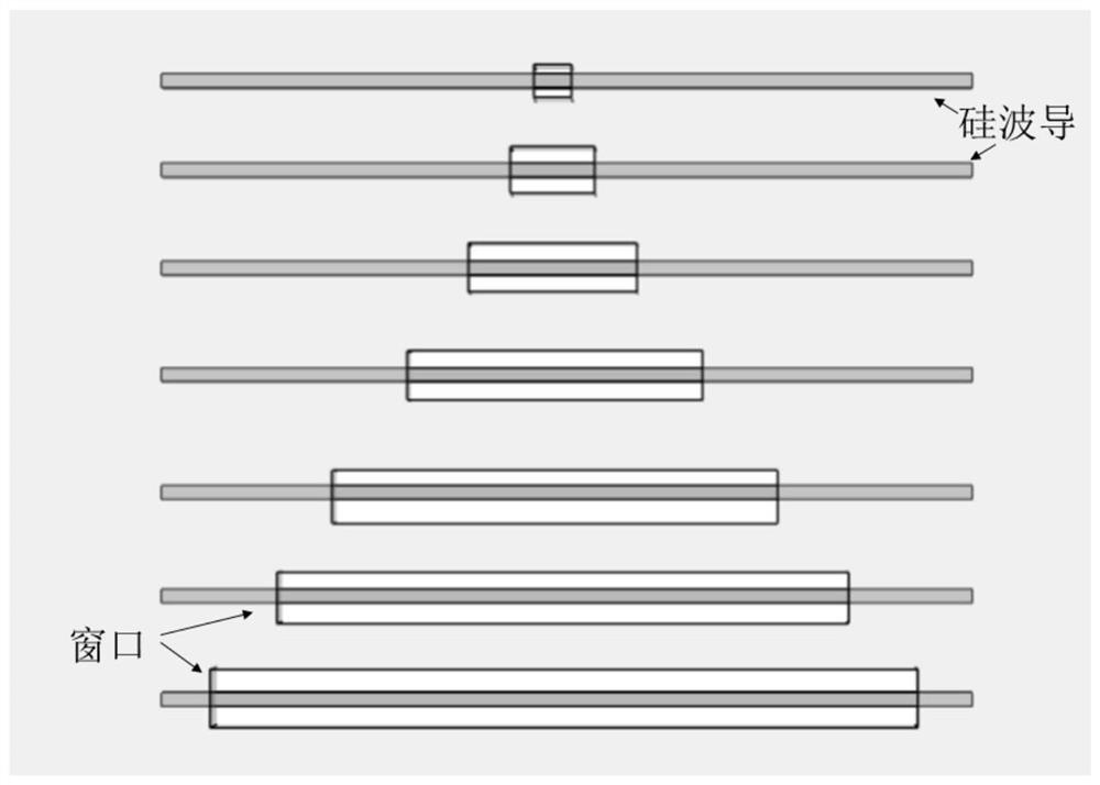
[0021] In order to accurately measure the optical loss of the thin film, the SOI substrate is patterned. The surface of the SOI substrate is cleaned with an organic solvent and deionized water, and the organic solvent includes acetone and ethanol. After exposure, development, and etching in sequence, a preset pattern such as figure 1 shown.
[0022] In order to obtain the underlying Si waveguide pattern and the cladding window pattern, two exposures, development, and etching are used. After exposure, development and etching for the first time, a Si waveguide pattern is obtained. After exposure, development and etching for the second time, a window pattern is formed on the waveguide.
[0023] Step 1: Deposit a layer of 10nm thick SiO on the SOI waveguide by sputtering 2 film. The sputtering power is 80W, the deposition rate is 1nm / min, the atm...
PUM
 Abstract
Description
Claims
Application Information


