
A kind of preparation method of single crystal vanadium dioxide thin film

A technology of vanadium dioxide and thin film, which is applied in the field of preparation of single crystal vanadium dioxide thin film, can solve the problems of high repeatability, high cost and harsh conditions, and achieve the effect of high repeatability, low annealing requirements and large deposition area

Active Publication Date: 2021-05-11
DONGHUA UNIV
View PDF3 Cites 0 Cited by
  • Summary
  • Abstract
  • Description
  • Claims
  • Application Information

AI Technical Summary

Problems solved by technology

[0005] The technical problem to be solved by the present invention is to provide a method for preparing a single crystal vanadium dioxide thin film, which overcomes the defects of the prior art preparation method such as harsh conditions and high cost. Low VO for single crystal 2 Easy Preparation of Thin Films

Method used


Image

  • A kind of preparation method of single crystal vanadium dioxide thin film
  • A kind of preparation method of single crystal vanadium dioxide thin film
  • A kind of preparation method of single crystal vanadium dioxide thin film

Examples


Embodiment 1

[0039] First, using the JPGF400B-G magnetron sputtering coating machine, using the method of DC magnetron sputtering on c-Al 2 o 3A metal vanadium thin film with extremely low resistivity is prepared on the substrate. The purity requirement of the magnetron sputtering metal vanadium target only needs to be greater than 99%, the target diameter is 60mm, the distance between the target and the substrate during magnetron sputtering coating is 180mm, and the substrate speed is 21.8rad / min; Pre-sputter the target for 15 minutes before coating, and then wait for the background vacuum to be 1.8×10 -3 After Pa is below, adjust the argon pressure to 1×10 -1 Under Pa, DC magnetron sputtering was carried out with a power of 140W for 5min.

[0040] The preparation parameters of the metal vanadium thin film are shown in Table 1 below:

[0041] Table 1 Preparation parameters of metal vanadium thin film

[0042] background vacuum Sputtering power sputtering gas Sputterin...

Embodiment 2

[0052] Directly give the specific preparation process using the traditional method, the traditional method: (refer to the patent a method for regulating the phase transition temperature of vanadium dioxide by rapid heat treatment, patent number: 201510824576.4, inventor: Liang Jiran, Li Jingpeng, Hou Luhui, Liu Xing).

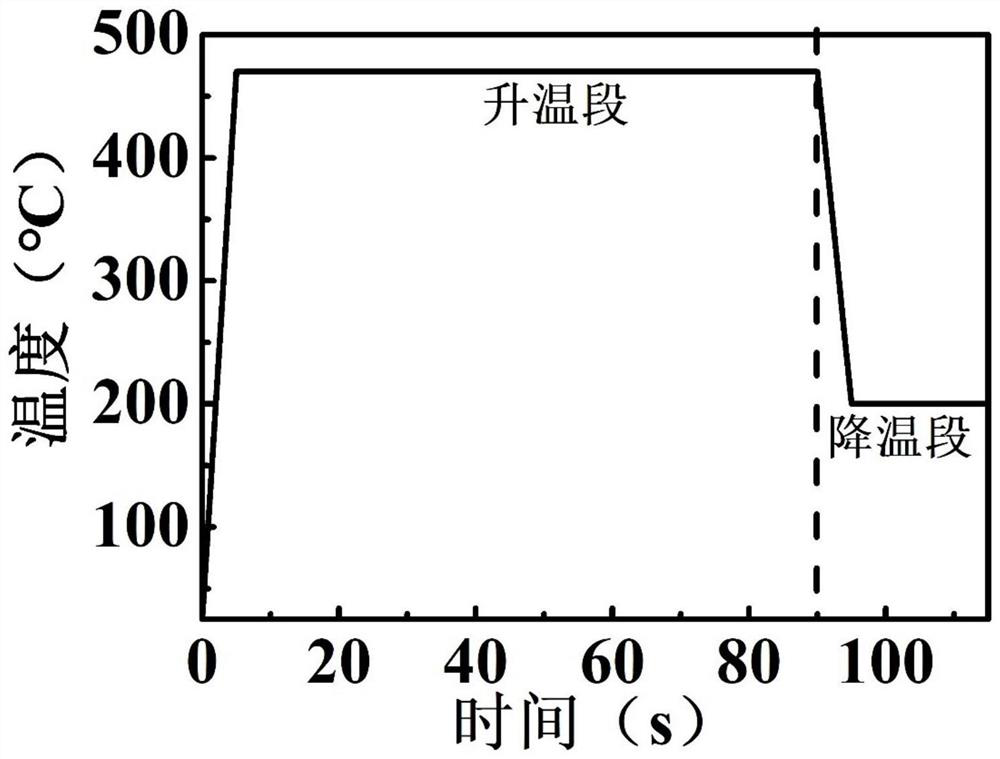
[0053] The sputtering pressure of metal vanadium thin film is 2×10 -0 Pa. The sputtering power is 75W, and the sputtering time is 10min-25min. After the end, the sample was taken out, the temperature was kept at 450°C, the heating time was 9s, the heating rate was 50°C / s, the holding time was 70s-170s, and the cooling time was 90s.

[0054] Result: the resistance-temperature change curve of embodiment 2 is as Image 6 As shown, the VO prepared by the traditional method 2 After the phase transition, the film can only achieve a change in the order of sheet resistance of about 3.1 orders of magnitude, the phase transition process is slow, and the hysteresis wid...


PUM

PropertyMeasurementUnit
diameteraaaaaaaaaa
thicknessaaaaaaaaaa
electrical resistivityaaaaaaaaaa

Abstract

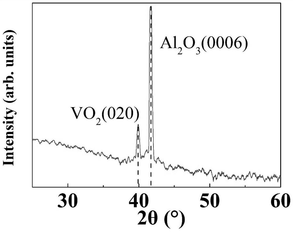
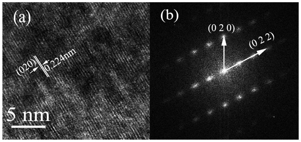
The present invention relates to a kind of preparation method of single crystal vanadium dioxide thin film, comprising: 2 o 3 Magnetron sputtering metal vanadium thin film on the substrate; then performing oxidation treatment in the air, cooling naturally, that is. The resistivity of the vanadium dioxide thin film prepared by the invention changes up to 4.6 orders of magnitude before and after the phase transition, and the crystallographic orientation of the thin film is (020) single crystal orientation. The invention provides a simple preparation method of single-crystal vanadium dioxide film, and is compatible with other semiconductor processes.

Description

technical field [0001] The invention belongs to the field of preparation of vanadium dioxide thin film materials, in particular to a preparation method of single crystal vanadium dioxide thin film. Background technique [0002] VO 2 Thin film is a kind of phase change material, which can realize ultrafast metal-insulator phase transition at about 68°C. VO 2 The physical properties of the thin film changed significantly before and after the phase transition, among which VO 2 The resistance of the film before and after the phase transition can change by several orders of magnitude. In particular, when VO with better crystallinity 2 Thin films grown on c-Al 2 o 3 When on the substrate, the ratio of the resistivity after the phase change to the resistivity before the phase change can exceed 4 orders of magnitude. This large change in resistivity before and after the phase transition not only reflects the VO 2 The good crystallinity of the film also makes the VO 2 Thin f...

Claims


Application Information

Patent Timeline
Patent Type & Authority Patents(China)
IPC IPC(8): C23C14/35
CPCC23C14/185C23C14/35C30B1/10C30B29/16C30B29/64
Inventor 徐晓峰蒙奕帆桑景新
Owner DONGHUA UNIV
Learn More