
Device with graphene and preparation method of device

A graphene and device technology, applied in the field of microelectronics, can solve problems such as poor adsorption capacity and poor light response capacity, and achieve the effects of increasing adsorption sites, strong repeatability, and stable and controllable growth process.

Inactive Publication Date: 2019-03-15
SHANGHAI INST OF MICROSYSTEM & INFORMATION TECH CHINESE ACAD OF SCI
View PDF5 Cites 0 Cited by
  • Summary
  • Abstract
  • Description
  • Claims
  • Application Information

AI Technical Summary

Problems solved by technology

[0003] In view of the above-mentioned shortcoming of the prior art, the object of the present invention is to provide a kind of device with graphene and preparation method thereof for solving the problems in the prior art due to poor graphene gas adsorption capacity and poor photoresponse ability

Method used


Image

  • Device with graphene and preparation method of device
  • Device with graphene and preparation method of device
  • Device with graphene and preparation method of device

Examples


Embodiment 1

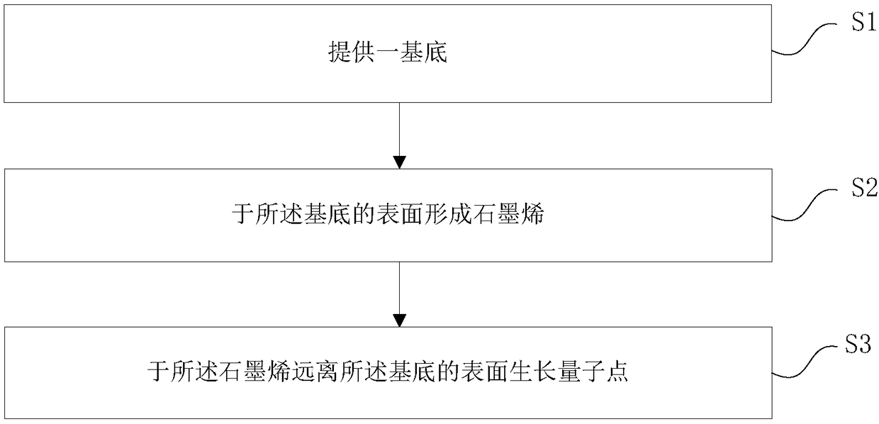
[0045] see figure 1 , the invention provides a kind of preparation method with the device of graphene, the preparation method of described device with graphene comprises the steps:

[0046] 1) Provide a base;

[0047] 2) forming graphene on the surface of the substrate;

[0048] 3) growing quantum dots on the surface of the graphene away from the substrate.

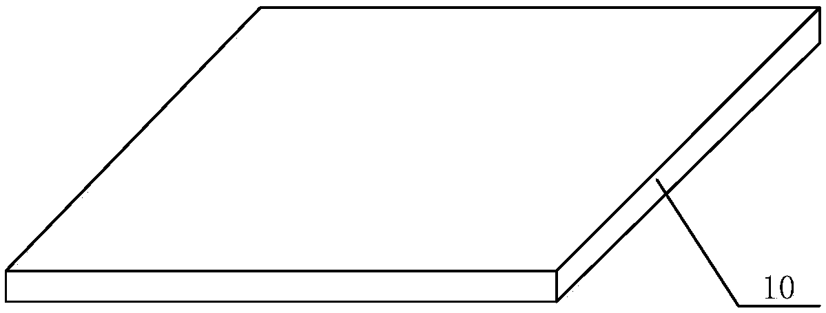
[0049] In step 1), see figure 1 Step S1 in and figure 2 , providing a substrate 10 .

[0050] As an example, the substrate 10 may include but not limited to a germanium (Ge) substrate; preferably, in this embodiment, the substrate 10 includes an N-type germanium substrate.

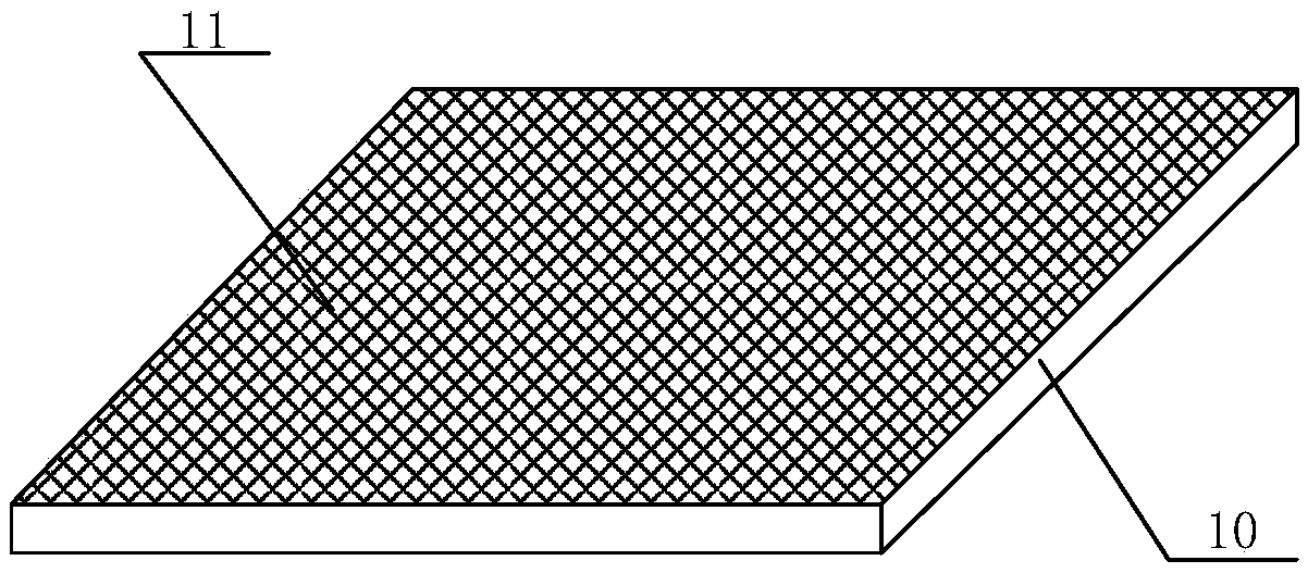
[0051] In step 2), see figure 1 Step S2 in and image 3 , forming graphene 11 on the upper surface of the substrate 10 .

[0052] As an example, the graphene 11 can be grown on the upper surface of the substrate 10 by using, but not limited to, a chemical vapor deposition (CVD) process.

[0053] As an example, the graphene 11 may include mon...

Embodiment 2

[0073] Please combine Figure 2 to Figure 5 read on Figure 4 and Figure 5 , the present invention also provides a device with graphene, the device with graphene comprising:

[0074] base 10;

[0075] Graphene 11, the graphene 11 is located on the surface of the substrate 10;

[0076] Quantum dots, the quantum dots are located on the surface of the graphene 11 away from the substrate 10 .

[0077] As an example, the substrate 10 may include but not limited to a germanium (Ge) substrate; preferably, in this embodiment, the substrate 10 includes an N-type germanium substrate.

[0078] As an example, the graphene 11 may include monoatomic layer graphene. Of course, in other examples, the graphene 11 may also be multi-atomic layer graphene. As a two-dimensional material, graphene has good electrical conductivity and very high carrier mobility, and is suitable as a channel material for photodetection.

[0079] As an example, the quantum dots can be germanium quantum dots 12...


PUM

PropertyMeasurementUnit
diameteraaaaaaaaaa
heightaaaaaaaaaa
heightaaaaaaaaaa

Abstract

The invention provides a device with graphene and a preparation method of the device. The preparation method of the device with the graphene comprises the following steps of 1) providing a substrate;2) forming the graphene on the surface of the substrate; and 3) growing quantum dots on the surface, away from the substrate, of the graphene. According to the preparation method of the device with the graphene, the quantum dots are grown through a molecular beam epitaxy process, and growth conditions of the molecular beam epitaxy process are adjusted, so that morphology features of the quantum dots epitaxially grown on the surface of the graphene can be effectively controlled; and the growth process is stable and controllable, is high in repeatability and is suitable to serve as a general method of graphene surface functionalization quantum dots.

Description

technical field [0001] The invention belongs to the technical field of microelectronics, in particular to a device with graphene and a preparation method thereof. Background technique [0002] Graphene is a hexagonal honeycomb two-dimensional nanostructure material composed of carbon atoms with sp2 hybrid orbitals. It has excellent photoelectric and mechanical properties and has important application prospects in many fields such as energy, materials, and biomedicine. However, the smooth surface of graphene has no dangling bonds, which is not conducive to effective gas adsorption. In addition, the excellent electrical properties of graphene lead to a large current of graphene itself, which is not conducive to the improvement of the responsivity of photodetector devices. Therefore, it is necessary to functionalize the surface of graphene. To enhance the gas adsorption and photoresponsive capabilities of graphene in order to improve the performance of graphene-based gas detect...

Claims


Application Information

Patent Timeline
Patent Type & Authority Applications(China)
IPC IPC(8): H01L31/18H01L31/028H01L31/0352H01L31/09
CPCH01L31/028H01L31/035218H01L31/09H01L31/1804Y02P70/50
Inventor 狄增峰杨悦昆刘冠宇郑鹏荣薛忠营张苗
Owner SHANGHAI INST OF MICROSYSTEM & INFORMATION TECH CHINESE ACAD OF SCI
Learn More