

Technological method for composite asynchronous polishing of ceramics using picosecond-nanosecond laser
A picosecond laser and process method technology, applied in laser welding equipment, manufacturing tools, metal processing equipment, etc., can solve the problems of easily damaged surface morphology, large amount of material removal, large thermal/mechanical stress affected area, etc., to achieve High surface activity and low melting point
- Summary
- Abstract
- Description
- Claims
- Application Information
AI Technical Summary
Problems solved by technology
Method used
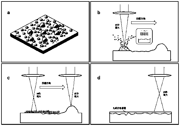
Image

Examples
Embodiment 1
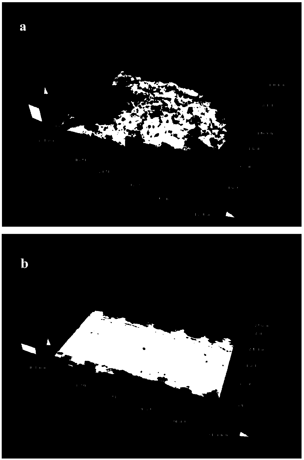
[0022] To polish the 95% alumina ceramic substrate, first use the picosecond laser with an average power of 60W, a repetition rate of 100,000KHz, and a defocus of 0 to start scanning irradiation, with a scanning speed of 400mm / s and a scanning path gap of 0.05mm. Sputtering used to remove material microscopic surface protrusions and excite micro-nano particles. After 50μs, the average power is 5W, the repetition frequency is 100KHz, and the nanosecond laser tracking the picosecond laser scanning path with a defocus of +0.3mm is irradiated at the same speed, which is used to melt the micro-nano particles produced by picosecond laser irradiation. It produces a layer of uniform and dense fine-grained fused layer. The used polishing process was taken out from the processing platform, and the surface micro-morphology was tested using a laser confocal microscope. The roughness Ra decreased from the original 1.70 μm to 0.68 μm. The three-dimensional surface morphology before and afte...
Embodiment 2
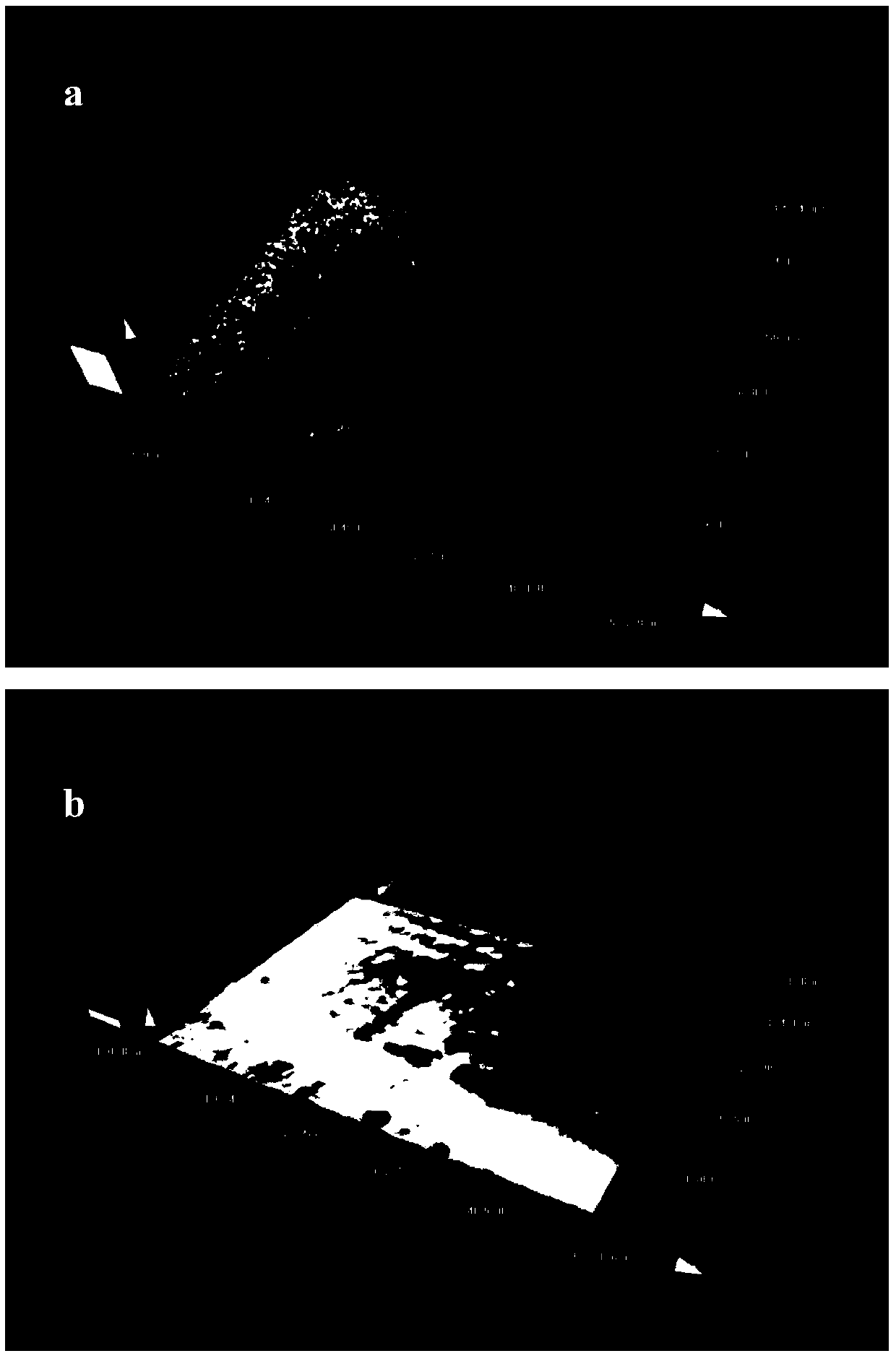
[0024] To polish the zirconia ceramic substrate, first use a picosecond laser with an average power of 30W, a repetition rate of 50,000KHz, and a defocus of 0 to start scanning irradiation. The scanning speed is 1000mm / s, and the scanning path gap is 0.01mm. , for sputtering to remove material microscopic surface protrusions and excite micro-nano particles. After 50μs, the average power is 3W, the repetition frequency is 50KHz, and the nanosecond laser tracking the picosecond laser scanning path with a defocus of +0.5mm is irradiated at the same speed, which is used to melt the micro-nano particles produced by picosecond laser irradiation, so that It produces a uniform dense fine-grained fused layer. The used polishing process was taken out from the processing platform, and the surface micro-morphology was tested using a laser confocal microscope. The roughness Ra decreased from the original 1.30 μm to 0.52 μm. The three-dimensional surface morphology before and after polishin...
Embodiment 3
[0026]To polish the aluminum nitride ceramic substrate, first use a picosecond laser with an average power of 55W, a repetition rate of 100,000KHz, and a defocus of 0 to start scanning irradiation, with a scanning speed of 300mm / s and a scanning path gap of 0.5mm. Sputtering used to remove microscopic surface protrusions and excite micro-nano particles of materials. After 100μs, the average power is 14W, the repetition frequency is 100KHz, and the nanosecond laser tracking picosecond laser scanning path is irradiated at the same speed with a defocus of +0.1mm, which is used to melt the micro-nano particles produced by picosecond laser irradiation, so that It produces a uniform dense fine-grained fused layer. The used polishing process was taken out from the processing platform, and the surface micromorphology was tested using a laser confocal microscope. The roughness Ra dropped from the original 1.81 μm to 0.65 μm.
PUM
| Property | Measurement | Unit |
|---|---|---|
| surface roughness | aaaaa | aaaaa |
| surface roughness | aaaaa | aaaaa |
| surface roughness | aaaaa | aaaaa |
Abstract
Description
Claims
Application Information