Flexible lead, preparation method of flexible electronic device and flexible wireless energy supply device

A technology of flexible wires and wires, which is applied in the field of electronics, can solve the problems of pollution, high price, and long time consumption in the natural environment, and achieve the effect of insensitivity to the external environment and high resource utilization.

Active Publication Date: 2019-03-29
TSINGHUA UNIV
View PDF3 Cites 12 Cited by
  • Summary
  • Abstract
  • Description
  • Claims
  • Application Information

AI Technical Summary

Problems solved by technology

[0008] First, special lithography machines and clean rooms are required and the process is cumbersome, the experimental conditions are high, the experimental preparation is difficult and time-consuming, and the experimental results in lithography are sensitive to the external environment, and multiple environmental parameters need to be controlled;
[0009] Second, the preparation process is a chemical treatment process, involving dangerous chemical reagents such as acetone, photoresist, and hydrofluoric acid. The waste liquid needs special treatment, which pollutes the natural environment;
[0010] Third, the photolithography process requires additional preparation of a special mask, and the pattern corresponding to each flexible wire needs to prepare a special mask, which is expensive and has a low utilization rate.

Method used


Image

  • Flexible lead, preparation method of flexible electronic device and flexible wireless energy supply device
  • Flexible lead, preparation method of flexible electronic device and flexible wireless energy supply device
  • Flexible lead, preparation method of flexible electronic device and flexible wireless energy supply device

Examples


preparation example Construction

[0063] When preparing the two-dimensional flexible wire, the preparation method includes a preparation step and a preparation step.

[0064] In the preparation step, a substrate is provided, which is formed by combining the rigid substrate, the sacrificial layer and the functional film.

[0065] In the preparation step:

[0066] Using femtosecond laser to cut the functional film of the above substrate to realize the patterning of the wires so that the functional film is formed with a planar wire structure;

[0067] Removal of the sacrificial layer so that the planar wire structure is separated from the rigid substrate;

[0068] The planar wire structure is formed as a two-dimensional flexible wire.

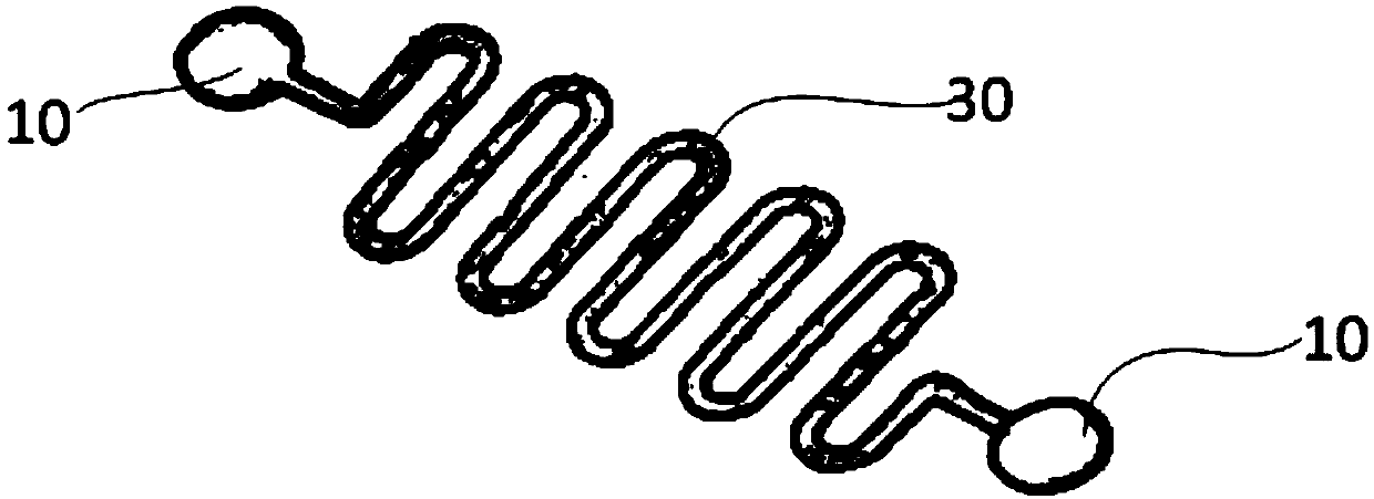
[0069] Such as figure 1 and figure 2 As shown, the planar wire structure of the two-dimensional flexible wire can have fixed regions and non-fixed regions. The fixed area can be fixed to the flexible substrate by sticking, so that the fixed area is formed as the sticking are...

no. 1 example

[0126] In this example, processing such as figure 1 and figure 2 The two types of conductors shown are serpentine conductors and parted serpentine conductors, such as Figure 4 As shown, the composition of the planar wire structure is: a sacrificial layer, a protective layer, a buffer layer, a functional layer and a protective layer arranged in sequence.

[0127] The sacrificial layer is made of polymethyl methacrylate (PMMA); the protective layer is made of PI with a thickness of 3 micrometers; the buffer layer is made of Cr with a thickness of 10 nanometers; the functional layer is made of gold thin film with a thickness of 200 nanometers.

[0128] Prepare a sacrificial layer, a protective layer and a functional film on a rigid substrate by spin coating and coating, and transfer the planar wire structure to a flexible substrate, including the following steps:

[0129] (1) Ultrasonic cleaning of the silicon wafer with acetone, ethanol, and deionized water for 10 min, cycle...

no. 2 example

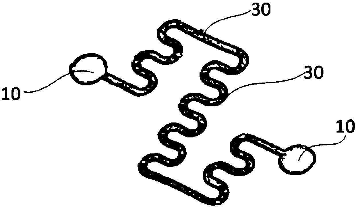
[0141] In this example, prepare as image 3 The helical 3D flexible wire shown and as Figure 5 Circuit shown with flexible wireless power device connected.

[0142] Such as Figure 4 As shown, the composition of the planar wire structure is: a sacrificial layer, a protective layer, a buffer layer, a functional layer and a protective layer arranged in sequence.

[0143] The sacrificial layer is made of PMMA; the protective layer is made of PI with a thickness of 3 microns; the buffer layer is made of Cr with a thickness of 10 nanometers; the functional layer is made of gold thin film with a thickness of 200 nanometers.

[0144] The sacrificial layer, protective layer and functional film are prepared on the rigid substrate by spin coating and coating method, and the planar wire structure is transferred to the pre-stretched flexible substrate, and the preparation of three-dimensional flexible wire is realized by buckling assembly technology. Including the following steps:

...


PUM

PropertyMeasurementUnit
thicknessaaaaaaaaaa

Abstract

The invention provides a flexible lead, a preparation method of a flexible electronic device and a flexible wireless energy supply device. The method comprises steps that a base material formed through combining a rigid substrate, a sacrificial layer and a functional film is provided; a femtosecond laser is utilized to cut the functional film of the base material such that the functional film is formed with a planar wire structure; the sacrificial layer is removed, and the planar wire structure is separated from the rigid substrate; a two-dimensional flexible wire is formed on the planar wirestructure; or the planar wire structure is assembled to a pre-stretched flexible substrate, pre-strain of the flexible substrate is released, and the planar wire structure is bent to form a three-dimensional flexible wire . The method is advantaged in that the flexible wire with high precision, large scale and no pattern limitation can be prepared, unique advantages of fast property, environmentalprotection, low cost, high resource utilization rate and insensitivity to the external environment can be further realized, and the method is suitable for preparing 2D and 3D flexible wires.

Description

technical field [0001] The disclosure relates to the field of electronic technology, in particular to a flexible wire, a method for preparing a flexible electronic device, and a flexible wireless energy supply device. Background technique [0002] In recent years, in order to meet people's needs for the flexibility of electronic devices, flexible electronic technology has developed rapidly, and many types of flexible electronic devices have emerged, such as flexible sensors, flexible displays, artificial electronic skins, and various wearable electronic products. . Among them, wearable electronic devices for health monitoring and medical treatment already have a trillion-level market. [0003] Wearable electronic devices can conform to the biological characteristics of the soft curved surface of human skin, and monitor human physiological signals more accurately and continuously. A large category of wearable electronic devices is inorganic flexible electronic devices, whic...

Claims


Application Information

Patent Timeline
Patent Type & Authority Applications(China)
IPC IPC(8): H01B5/14H01B13/00H01Q1/38H01Q1/50H01Q7/00H01Q21/00H02J50/20
CPCH01B5/14H01B13/00H01Q1/38H01Q1/50H01Q7/00H01Q21/0006H01Q21/0087H02J50/20
Inventor 张一慧程旭宋洪烈
Owner TSINGHUA UNIV
Why Eureka
Try Eureka