Microporous array processing device and microporous array processing method

A microhole array and processing method technology, applied in the direction of microstructure devices, metal processing equipment, manufacturing tools, etc., can solve the problems of affecting processing efficiency, inability to process multiple microholes at the same time, affecting productivity, etc., to improve work efficiency , small thermal impact, and the effect of improving quality

Inactive Publication Date: 2019-04-05
SHANGHAI MICRO ELECTRONICS EQUIP (GRP) CO LTD
View PDF7 Cites 20 Cited by
  • Summary
  • Abstract
  • Description
  • Claims
  • Application Information

AI Technical Summary

Problems solved by technology

[0003] like figure 1 As shown, the prior art discloses a laser microhole array processing device, including a laser system 1 arranged in sequence along the light propagation direction for generating laser light; a half-wave plate and a polarization 2 for adjusting laser energy; a pyramid Prism 3 is used to produce Bessel spot; Reflector 5; Plano-convex lens 4 and focusing objective lens 6 form telescopic system, described Bessel beam is narrowed into micro-Bessel beam; Motion table 7 is used for placing and Adjust the components to be processed. This device mainly processes the microhole array through the high-speed movement of the moving table 7, but only one hole is processed at a time, an

Method used


Image

  • Microporous array processing device and microporous array processing method
  • Microporous array processing device and microporous array processing method
  • Microporous array processing device and microporous array processing method

Examples


Embodiment 1

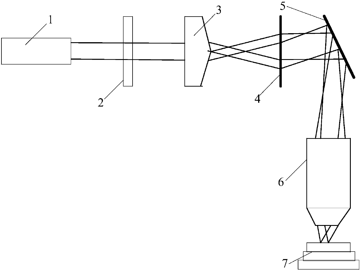
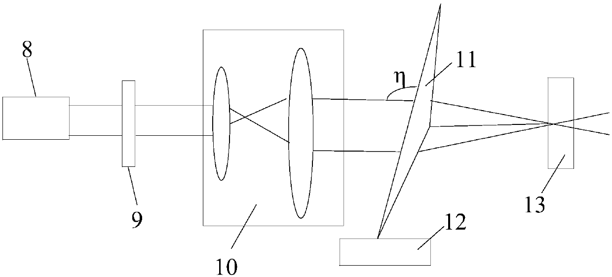
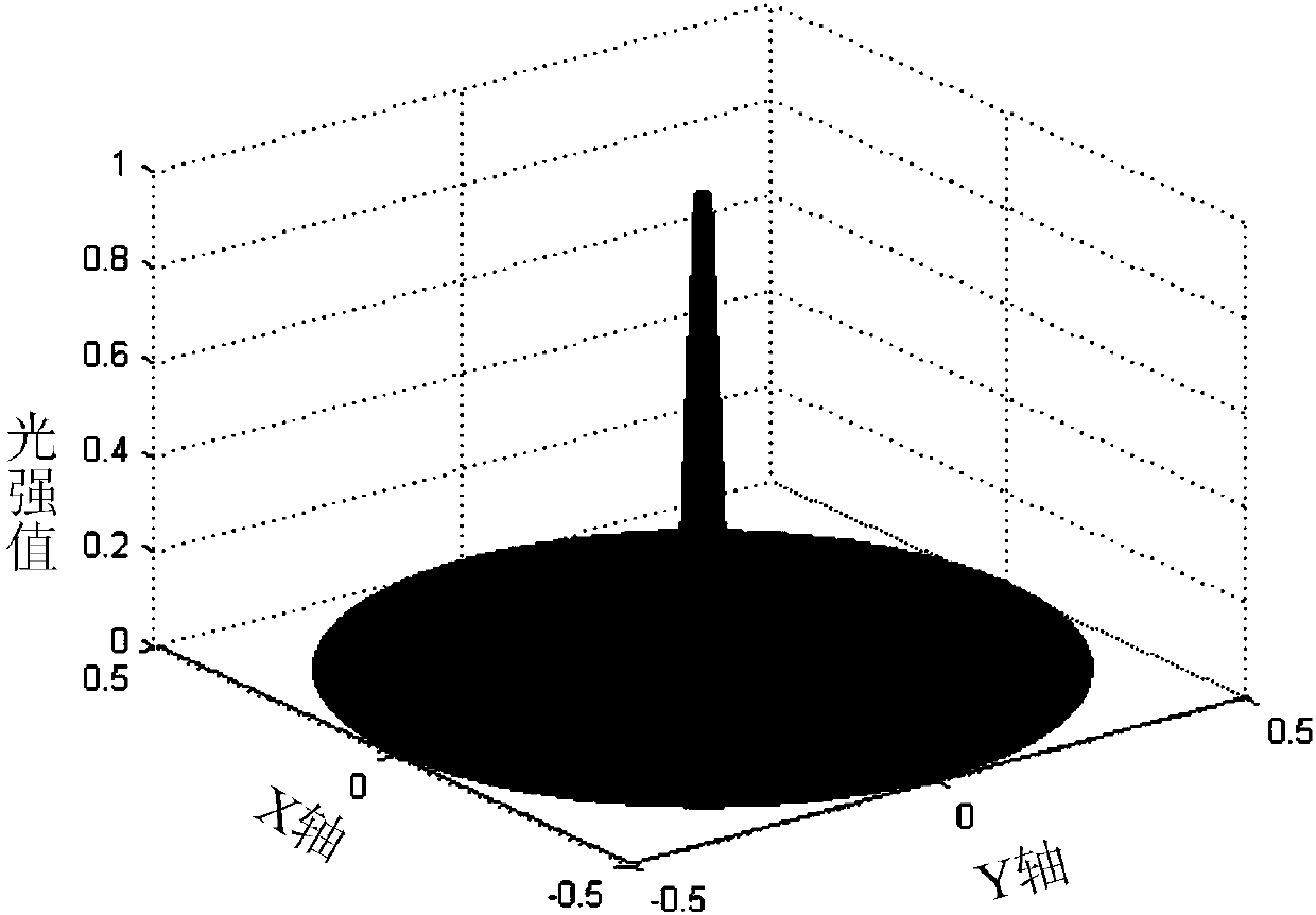
[0048] Such as figure 2 As shown, the present invention provides a microhole array processing device comprising: a laser, a light source adjustment assembly, an axicon 11, and a three-dimensional motion table 13 are sequentially arranged along the light propagation direction, and the axicon 11 is installed on a rotary table 12; The laser of the embodiment is preferably a femtosecond laser 8, which produces a femtosecond laser, which has the advantages of short action time, less thermal influence, little influence on the strength of the processed material, and no microcracks; the rotating table 12 is preferably five The axial precision rotary table can drive the axicon 11 to continuously change the angle. Specifically, the femtosecond laser 8 emits laser light and enters the axicon 11 to form a Bessel spot, and a computer program is used to control the movement of the three-dimensional motion table 13, so that the Bessel The Er area is located on the surface of the component t...

Embodiment 2

[0070] The difference between this embodiment and Embodiment 1 is that the number and distribution of light spots corresponding to the microhole array required by the element to be processed are obtained by adjusting the distance between the light field distribution plane and the axicon, as follows:

[0071] The N value is obtained by solving the light field distribution function: N=kz(n-1) 2 gamma 2 sin 2 η / 4, the specific decomposing steps have been listed in detail in Example 1, and will not be repeated in this example. It can be seen that N directly affects the light field distribution and the value of N is closely related to the angle n between the laser beam and the axicon 11 and the distance between the light field distribution plane and the axicon 11, the present embodiment will After the microhole array required by the component to be processed is substituted into the light field distribution function, the angle between the laser beam and the axicon 11 is 90°, and t...


PUM


Abstract

The invention discloses a microporous array processing device and a microporous array processing method. The microporous array processing method comprises the following steps of S1, converting a laserbeam into Bessel spots by means of an axicon principle, and focusing the spots to the surface of a to-be-processed component; S2, adjusting the axicon according to a microporous array needed by the to-be-processed component to obtain quantity and distribution of the needed spots; and S3, processing the spots to the to-be-processed component by means of laser pulse to form the microporous array. The microporous array processing device comprises a laser light source, a light source adjusting assembly, the axicon and a moving table successively arranged along the direction of propagation of light, wherein the axicon is mounted on a five-axis precision rotary table and is driven by the five-axis precision rotary table to adjust the angle the axicon and an incident beam. The microporous arrayprocessing device and the microporous array processing method process multiple micropores at single time, so that the work efficiency is improved. The heat effect is relatively long, the action of pulse laser is small, and the quality of a processed material is improved.

Description

technical field [0001] The invention relates to the field of microhole array processing, in particular to a microhole array processing device and method. Background technique [0002] The processing and manufacturing of micropores plays an extremely important role in related fields such as aviation, aerospace, and microfluidic devices. With the continuous development of laser technology, it is of great practical significance to apply laser technology to micropore manufacturing. Laser microhole manufacturing overcomes the influence of mutual contact of previous mechanical processing technologies, and will not cause mechanical damage to the processed material, nor will it cause fracture damage due to the hardness of the processed material, so it has a good application prospect. [0003] Such as figure 1 As shown, the prior art discloses a laser microhole array processing device, including a laser system 1 arranged in sequence along the light propagation direction for generati...

Claims


Application Information

Patent Timeline
IPC IPC(8): B23K26/382B81C99/00
CPCB23K26/382B81C99/00B81C99/001
Inventor 林圆圆
Owner SHANGHAI MICRO ELECTRONICS EQUIP (GRP) CO LTD
Why Eureka
Try Eureka