Waveguide phase shifter and preparation method thereof

A technology of phase shifter and waveguide, which is applied in the field of waveguide phase shifter and its preparation, can solve the problems of limited phase adjustment and difficult application, and achieve the effect of separation, high yield and high-precision scanning

Inactive Publication Date: 2019-04-05
BEIJING WANJI TECH
View PDF3 Cites 5 Cited by
  • Summary
  • Abstract
  • Description
  • Claims
  • Application Information

AI Technical Summary

Problems solved by technology

[0005] The embodiment of the present invention provides a waveguide phase shifter and its preparation method, which is used to solve the problem that the waveguide phase shifter using the thermo-optic effect in the prior art has limited phase adjustment and is difficult to apply in practice

Method used


Image

  • Waveguide phase shifter and preparation method thereof
  • Waveguide phase shifter and preparation method thereof
  • Waveguide phase shifter and preparation method thereof

Examples


preparation example Construction

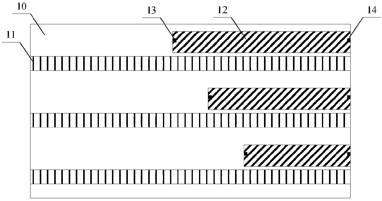
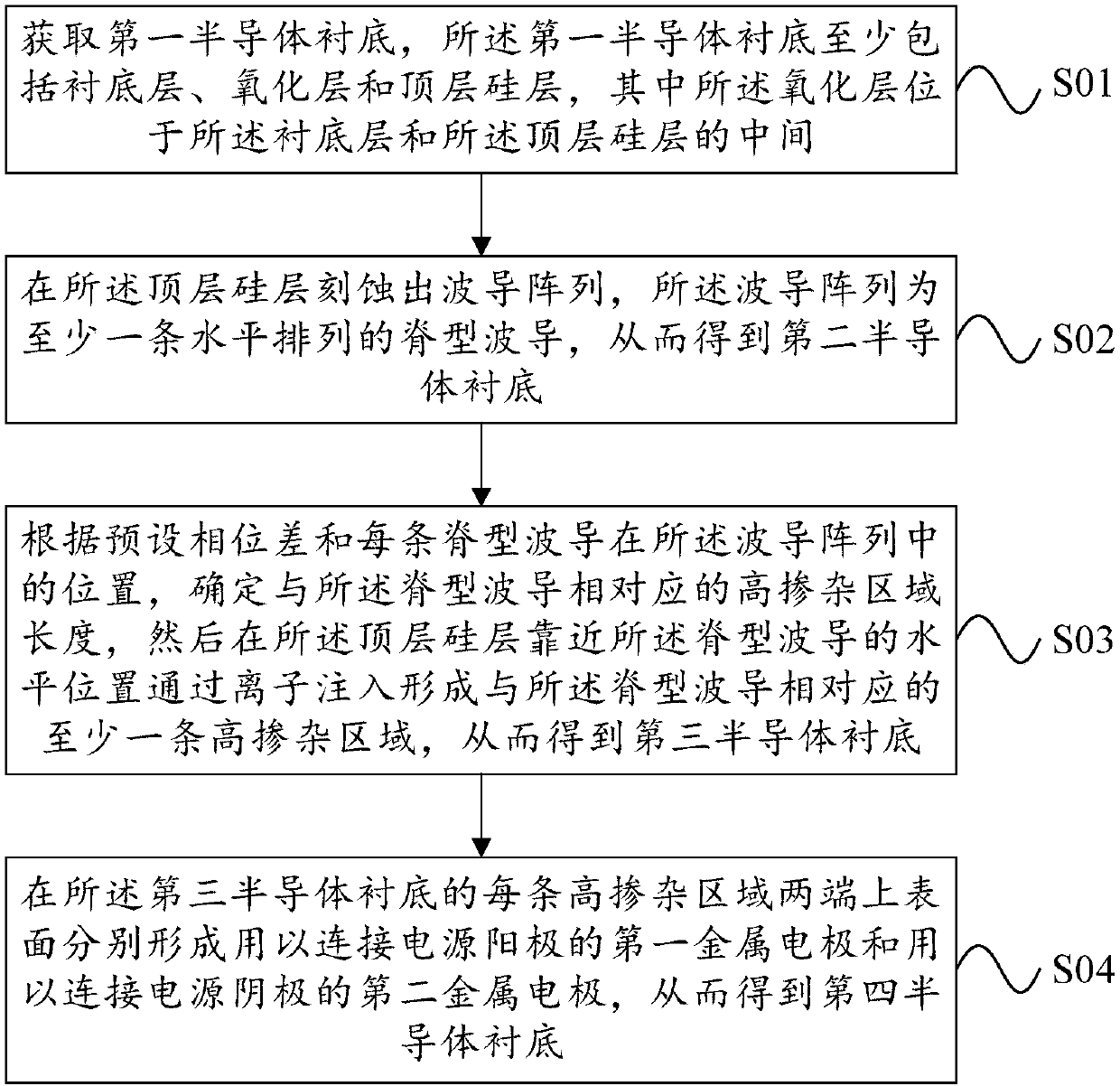
[0043] figure 2 It is a schematic flow chart of a method for preparing a waveguide phase shifter according to an embodiment of the present invention, image 3 It is a schematic diagram of the structure of the first semiconductor substrate according to the embodiment of the present invention, Figure 4 It is a schematic diagram of the structure of the second semiconductor substrate according to the embodiment of the present invention, Figure 5 is a schematic structural diagram of a third semiconductor substrate according to an embodiment of the present invention, Figure 6 It is a schematic diagram of the structure of the fourth semiconductor substrate according to the embodiment of the present invention, such as figure 2 As shown, the method includes:

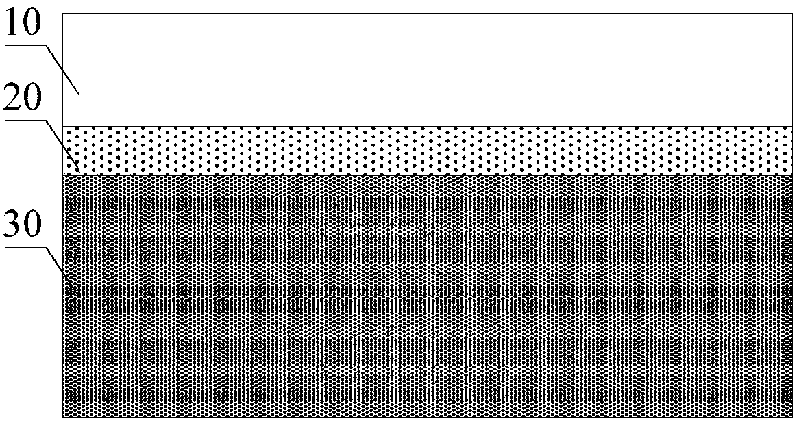
[0044] Step S01, obtaining a first semiconductor substrate, the first semiconductor substrate at least including a substrate layer, an oxide layer and a top silicon layer, wherein the oxide layer is located between the su...


PUM


Abstract

Embodiments of the invention provide a waveguide phase shifter and a preparation method thereof. The waveguide phase shifter comprises a semiconductor substrate comprising at least a substrate layer,an oxide layer, and a top silicon layer. The oxide layer is located between the substrate layer and the top silicon layer. A waveguide array is etched the on the top silicon layer. The waveguide arrayis at least one horizontally arranged ridge waveguide, and at least one highly doped region corresponding to the ridge waveguide is formed by ion implantation at a horizontal position of the top silicon layer close to the ridge waveguide. A first metal electrode for connecting power source anode and a second metal electrode for connecting power source cathode are respectively formed on upper surfaces at both ends of each highly doped region. The waveguide phase shifter provided by the embodiments of the invention provides a heated highly doped region on the side of the ridge waveguide, thereby realizing phase modulation of light wave passing through the ridge waveguide, which improves the heating efficiency of the ridge waveguide and improves the adjustment range of the phase.

Description

technical field [0001] Embodiments of the present invention relate to the technical field of optical semiconductors, in particular to a waveguide phase shifter and a manufacturing method thereof. Background technique [0002] Lidar is a radar system that emits laser beams to detect characteristic quantities such as the position and speed of targets. Its working principle is similar to microwave radar. Obtain multi-channel lasers with equal phase intervals through the phase shifter array, so as to control the direction of the outgoing light and send detection signals to the target, and then compare the received signal reflected from the target, that is, the target echo with the transmitted signal, through the software Processing can accurately obtain the target distance, azimuth, height, speed, shape and other parameters, so as to detect, track and identify the target. The development of artificial intelligence, the rise of autonomous driving and assisted driving will great...

Claims


Application Information

Patent Timeline
Patent Type & Authority Applications(China)
IPC IPC(8): G02F1/01G02F1/015
CPCG02F1/0147G02F1/015G02F1/01
Inventor 郑军徐洋李传波王庆飞田林岩
Owner BEIJING WANJI TECH
Why Eureka
Try Eureka