Preparation method and light-emitting device of modified metal chalcogenide

A metal sulfur compound technology, applied in the preparation method of modified metal chalcogenides and the field of light-emitting devices, can solve the problems of poor hole transport ability, achieve high charge transport efficiency, low cost, and realize the effect of large-scale production

Active Publication Date: 2020-01-03
TCL CORPORATION
View PDF3 Cites 0 Cited by
  • Summary
  • Abstract
  • Description
  • Claims
  • Application Information

AI Technical Summary

Problems solved by technology

[0004] The purpose of the present invention is to provide a method for preparing a modified metal chalcogenide and a light-emitting device, aiming to solve the problem that the existing metal chalcogenide has many defects and defect states when it is used as a hole transport material. The problem of poor hole transport ability

Method used


Image

  • Preparation method and light-emitting device of modified metal chalcogenide
  • Preparation method and light-emitting device of modified metal chalcogenide
  • Preparation method and light-emitting device of modified metal chalcogenide

Examples


preparation example Construction

[0016] The embodiment of the present invention provides a preparation method of a modified metal chalcogenide. This preparation method comprises the steps:

[0017] Step S11: providing a metal chalcogenide, and placing the metal chalcogenide in a reaction chamber.

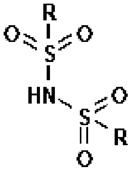
[0018] In the embodiment of the present invention, the chemical formula of the metal chalcogenide is generally MS 2 , where M is a metal element, such as Mo, W, V, Nb, Ta, etc., and S represents chalcogen elements such as S and Se. The prepared metal chalcogenides are placed in a reaction chamber for processing, and the reaction chamber is a device that can be ventilated and can be sealed.

[0019] Step S12: Passing in a non-oxidizing acid to perform a first modification treatment on the metal chalcogenide.

[0020] In an embodiment of the present invention, feeding the non-oxidizing acid includes: feeding an inert gas into the non-oxidizing acid solution, and letting the inert gas flow into the reaction chamber...

Embodiment 1

[0052] (1) Deposit a layer of MoS on a substrate containing silver nanowires 2 , by spin coating (NH 4 ) 2 MoS 4 aqueous solution and then heated and annealed to obtain MoS 2 Thin film (wherein, the heating condition is: 80°C / 15min in air, and the annealing condition is: inert gas annealing 300°C / 15min);

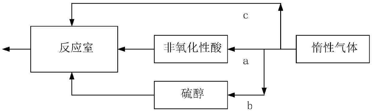
[0053] (2) MoS 2 film into the figure 2 In the device, the first modification treatment and the second modification treatment are carried out. Firstly, the gas HI of path a is introduced, and after 15 minutes of ventilation, the path a is closed, and the inert gas is introduced through path c to increase the pressure, and the pressure is 5 MPa. After the pressure is lowered to normal pressure, the gas ethanedithiol is introduced into route b, and after ventilation for 15 minutes, an inert gas is introduced through route c to increase the pressure, and the pressure is 5MPa. After the pressure is reduced to normal pressure, move the substrate into the glove box, deposi...

Embodiment 2

[0058] (1) Deposit a layer of MoSe on the substrate containing FTO 2, the thickness of 20nm was prepared by CVD method, and then the MoSe 2 film into the image 3 The first modification treatment and the second modification treatment are carried out in the device. First pass the gas HBr into the a channel, and after 30 minutes of ventilation, close the a channel, and feed the inert gas through the c channel to increase the pressure, and the pressure is 5MPa. After the pressure is lowered to normal pressure, ethanedithiol is introduced into route b, and after ventilation for 15 minutes, an inert gas is introduced through route c to increase the pressure, and the pressure is 5MPa. After the pressure is reduced to normal pressure, the substrate is moved into the glove box, and then a layer of hole transport layer is deposited, which is TFB, which is spin-coated at a speed of 3000rpm, and then annealed at 150°C for 30min;

[0059] (2) Deposit a layer of light-emitting layer wit...


PUM

PropertyMeasurementUnit
carrier mobilityaaaaaaaaaa
thicknessaaaaaaaaaa
thicknessaaaaaaaaaa

Abstract

The invention belongs to the field of display devices and provides a preparation method of a modified metal chalcogen compound and a light emitting device. In the present invention, the metal chalcogen compound is provided, and the metal chalcogen compound is placed in a reaction chamber to perform the first modification treatment and the second modification treatment to obtain the modified metal chalcogen compound. In this preparation process, the first modification treatment reduces the defects of chalcogen elements through sufficient acid treatment, and releases the charges combined with the defect states of chalcogen elements, and at the same time removes the oxygen species (oxygen species) to obtain purer metal chalcogenides; the second modification treatment allows chalcogen defect states and thiols to chemically adsorb in the form of covalent bonds through thiol treatment, and eliminates the remaining defects on the surface of chalcogens to the minimum; thereby obtaining a modified metal chalcogenide with higher charge transport efficiency, which improves the luminous efficiency of the device. In addition, the preparation method has simple process and low cost, and can realize large-scale production.

Description

technical field [0001] The invention belongs to the field of display devices, in particular to a preparation method of a modified metal chalcogenide compound and a light emitting device. Background technique [0002] In the existing preparation technology of QLED and OLED, organic materials are usually used as hole transport materials, commonly used PEDOT:PSS, however, the acidity and easy water absorption of the EDOT:PSS hole injection layer have caused different degrees of damage to ITO and devices. Damage and attenuation, so the stability of the device needs to be improved. In the current reports on replacing PEODT:PSS, metal oxides are often used as substitutes, such as molybdenum oxide, nickel oxide or copper oxide; and in other reports on solar cells, metal chalcogenides are also used. to replace PEDOT:PSS, such as molybdenum sulfide and copper sulfide. Sulfides have high carrier mobility (200cm 2 ·V -1 ·s -1 -500cm 2 ·V -1 ·s -1 ) are widely used in photocatal...

Claims


Application Information

Patent Timeline
Patent Type & Authority Patents(China)
IPC IPC(8): H01L51/56H01L51/50H01L51/54
CPCH10K50/155H10K2102/00H10K71/00
Inventor 王宇曹蔚然李龙基
Owner TCL CORPORATION
Why Eureka
Try Eureka