

P-type phosphorus-doped two-dimensional tungsten selenide semiconductor material and preparation method thereof
A tungsten diselenide and phosphorus doping technology, which is applied in the direction of binary selenium/tellurium compounds, metal selenide/telluride, etc., can solve the problems of small crystal domain size and low quality, reduce evaporation temperature and improve product quality. quality, growth-promoting effect
- Summary
- Abstract
- Description
- Claims
- Application Information
AI Technical Summary
Problems solved by technology
Method used
Image

Examples
Embodiment 1
[0031] The preparation method of the p-type phosphorus-doped two-dimensional tungsten diselenide semiconductor material of this embodiment includes the following steps:
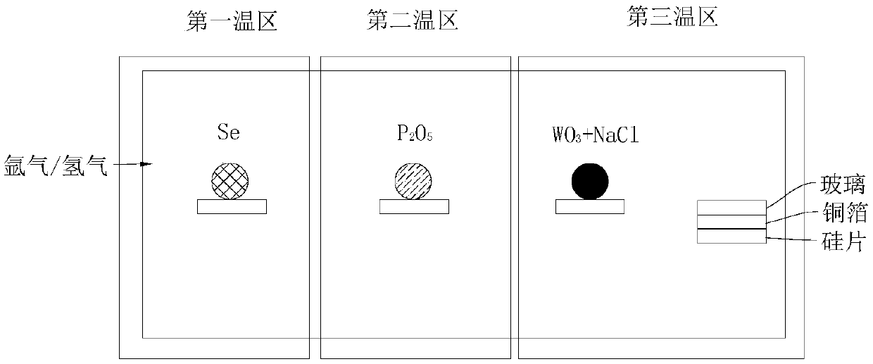
[0032] (1) 100 parts of Se element, P 2 O 5 30 copies and WO 3 30 parts of the mixture of NaCl and NaCl are respectively placed on the silicon wafer, and then put into the first temperature zone, the second temperature zone and the third temperature zone of the reaction furnace, and in the third temperature zone according to figure 1 Insert the growth substrate as shown, and the substrate is loaded with P 2 O 5 The distance between the silicon wafers is 5cm. Among them, WO 3 The mass ratio to NaCl is 5:1, and the substrate is stacked from bottom to top in the order of silicon wafer, copper foil and soda lime glass.
[0033] (2) Pass in 100sccm of argon gas, heat up the above three temperature zones to 100°C at a rate of 35°C / min, and hold for 10 minutes to remove the H that may be adsorbed in the CVD system 2 O; ...
Embodiment 2
[0036] The preparation method of the p-type phosphorus-doped two-dimensional tungsten diselenide semiconductor material of this embodiment includes the following steps:
[0037] (1) 50 parts of Se element, P 2 O 5 20 copies and WO 3 30 parts of the mixture of NaCl and NaCl are respectively placed on the silicon wafer, and then put into the first temperature zone, the second temperature zone and the third temperature zone of the reaction furnace, and in the third temperature zone according to figure 1 Insert the growth substrate as shown, and the substrate is loaded with P 2 O 5 The distance between the silicon wafers is 10cm. Among them, WO 3 The mass ratio to NaCl is 5:1, and the substrate is stacked from bottom to top in the order of silicon wafer, copper foil and soda lime glass.
[0038] (2) Pass in 100sccm of argon gas, heat up the above three temperature zones to 100°C at a rate of 35°C / min, and hold for 10 minutes to remove the H that may be adsorbed in the CVD system 2 O; T...
Embodiment 3
[0041] The preparation method of the p-type phosphorus-doped two-dimensional tungsten diselenide semiconductor material of this embodiment includes the following steps:
[0042] (1) 100 parts of Se element, P 2 O 5 10 copies and WO 3 30 parts of the mixture of NaCl and NaCl are respectively placed on the silicon wafer, and then put into the first temperature zone, the second temperature zone and the third temperature zone of the reaction furnace, and in the third temperature zone according to figure 1 Insert the growth substrate as shown, and the substrate is loaded with P 2 O 5 The distance between the silicon wafers is 20cm. Among them, WO 3 The mass ratio to NaCl is 5:1, and the substrate is stacked from bottom to top in the order of silicon wafer, copper foil and soda lime glass.
[0043] (2) Pass in 100sccm of argon gas, heat up the above three temperature zones to 100°C at a rate of 35°C / min, and hold for 10 minutes to remove the H that may be adsorbed in the CVD system 2 O;...
PUM
 Abstract
Description
Claims
Application Information