

Ultra-wide-band wave absorbing structure integrating temperature resistance and mechanical properties and preparation method of ultra-wide-band wave absorbing structure
An ultra-wideband, wave-structured technology, applied in chemical instruments and methods, laminated, layered products, etc., can solve the problems of poor stealth performance of ultra-low frequency, can not be applied to high-speed flight environment, etc., achieves strong designability, solves problems of radar The stealth problem, the effect of solving the ultra-wideband stealth problem compatible with temperature resistance and mechanical properties
- Summary
- Abstract
- Description
- Claims
- Application Information
AI Technical Summary
Problems solved by technology
Method used
Image

Examples
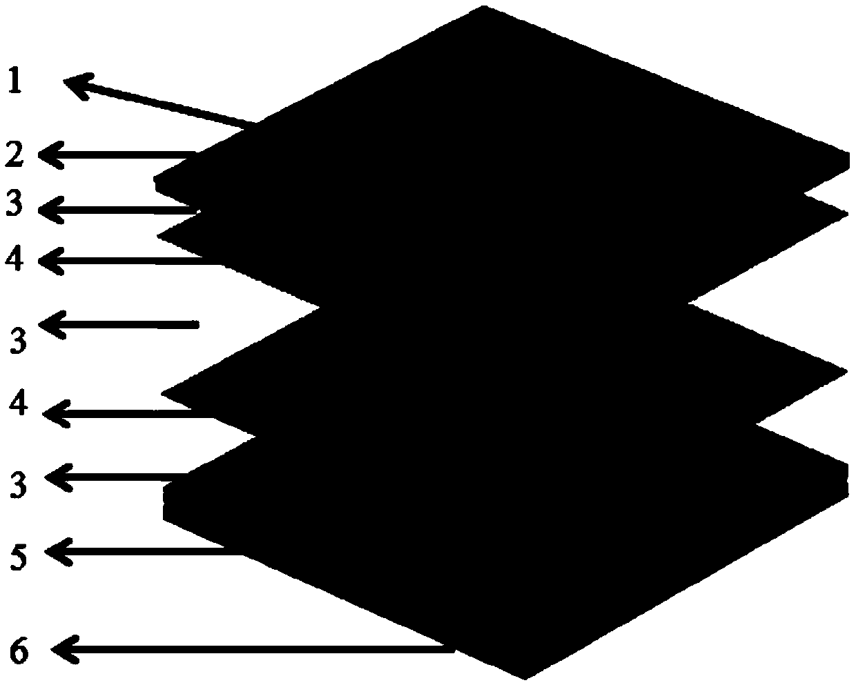
Embodiment 1
[0042] Step 1: Prepare the electromagnetic shielding layer
[0043] Two-dimensional laminated shielding SiC fibers (the real part of the dielectric constant is >20) are selected as the prefabricated body of the electromagnetic shielding layer, and the rough blank is prepared by the fiber impregnation and pyrolysis process (PIP). After the braid has sufficient strength and toughness, pass The electromagnetic shielding layer is obtained by machining.
[0044] Step 2: Prepare the magnetic wave-absorbing patch layer
[0045] Pour vulcanized polyurethane rubber and micron magnetic iron powder (60wt.%) into an open mill and knead evenly. The kneading temperature is 25°C-60°C, and the above-mentioned mixture is pressed into a wave-absorbing layer with a thickness of 0.3-3mm by a calender. Raw film, cut into the designed shape, put it into the mold, heat up and vulcanize after closing the mold, and obtain the required magnetic wave-absorbing patch material, its dielectric constant an...
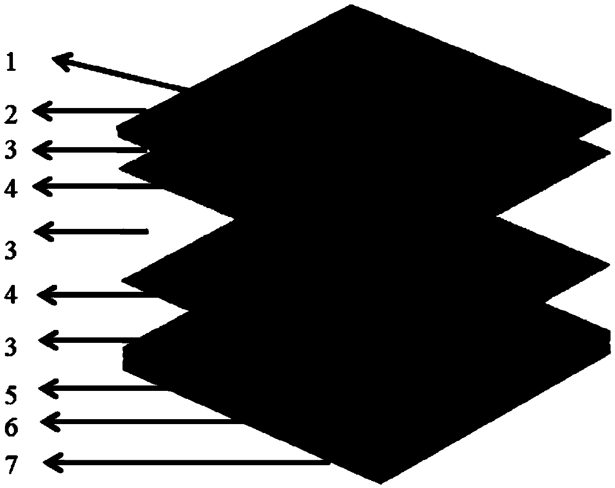
Embodiment 2
[0057] Step 1: Prepare the electromagnetic shielding layer
[0058] The two-dimensional laminated T300 carbon fiber (conductivity is about 40000S / m) is selected as the prefabricated body of the electromagnetic shielding layer. After the braid has sufficient strength and toughness, the electromagnetic shielding layer is obtained by machining.
[0059] Step 2: Prepare precursors containing magnetic absorbers
[0060] Using micron magnetic iron-nickel alloy powder (75wt.%) as the wave absorbing agent and silica sol as the solvent, the wave absorbing agent and the solvent are fully mixed by mechanical stirring and ultrasonic dispersion to form a slurry to prepare the bottom magnetic wave absorbing material layer.
[0061] The third step: preparation of ceramic matrix composite material layer
[0062] The ceramic matrix composite layer is made of Al 2 o 3 Fiber reinforced Al 2 o 3 Ceramic matrix composite material, choose Al 2 o 3 The fiber is braided to obtain a fiber prefo...
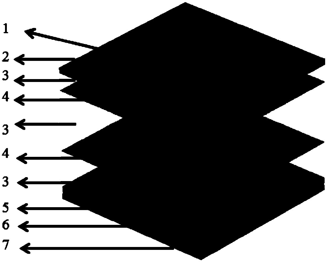
Embodiment 3
[0074] Step 1: Prepare the electromagnetic shielding layer
[0075] The two-dimensional laminated T300 carbon fiber (conductivity is about 40000S / m) is selected as the prefabricated body of the electromagnetic shielding layer. After the braid has sufficient strength and toughness, the electromagnetic shielding layer is obtained by machining.
[0076] Step 2: Prepare precursors containing magnetic absorbers
[0077] Using micron iron powder (75wt.%) as wave absorbing agent, Al 2 o 3 The precursor is a solvent, and the wave absorbing agent and solvent are fully mixed by mechanical stirring and ultrasonic dispersion to form a slurry to prepare the bottom magnetic wave absorbing material.
[0078] The third step: preparation of ceramic matrix composite material layer
[0079] The ceramic matrix composite material is made of silicon nitride fiber reinforced silicon nitride ceramic matrix composite material, and the silicon nitride fiber is used for weaving to obtain a fiber pref...
PUM
| Property | Measurement | Unit |
|---|---|---|
| thickness | aaaaa | aaaaa |
| thickness | aaaaa | aaaaa |
| electrical conductivity | aaaaa | aaaaa |
Abstract
Description
Claims
Application Information