Metal-insulator-semiconductor transistors with gate-dielectric/semiconductor interfacial protection layer

A gate dielectric layer and interface protection technology, applied in semiconductor devices, semiconductor/solid-state device manufacturing, circuits, etc., can solve the threshold voltage stability gate dielectric reliability hinders the commercialization of gate E-mode III-NMIS-FET , small safe operating range and other issues, to achieve the effects of high stability, small hysteresis, and high threshold voltage stability

Inactive Publication Date: 2019-04-26
THE HONG KONG UNIV OF SCI & TECH
View PDF2 Cites 3 Cited by
  • Summary
  • Abstract
  • Description
  • Claims
  • Application Information

AI Technical Summary

Problems solved by technology

[0006] However, threshold voltage stability and gate dielectric reliability issues have been hindering the commercialization of recessed gate E-mode III-N MIS-FETs despite enhanced gate swing and lower gate leakage current.
This results in a smaller safe operating range for the gate bias of p-GaNE mode devices
[0009] The above analysis of conventional III-nitride based devices is only intended to outline some of the problems with conventional systems and methods, and is not intended to be exhaustive

Method used


Image

  • Metal-insulator-semiconductor transistors with gate-dielectric/semiconductor interfacial protection layer
  • Metal-insulator-semiconductor transistors with gate-dielectric/semiconductor interfacial protection layer
  • Metal-insulator-semiconductor transistors with gate-dielectric/semiconductor interfacial protection layer

Examples


no. 1 example

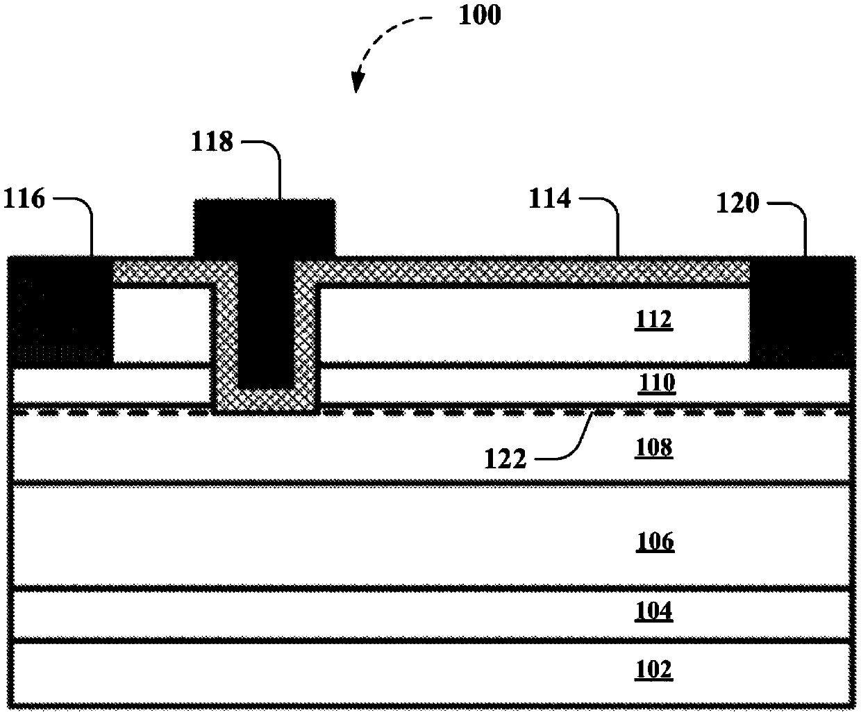
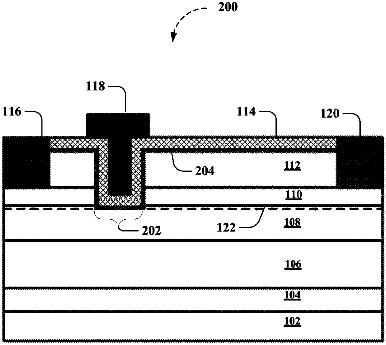
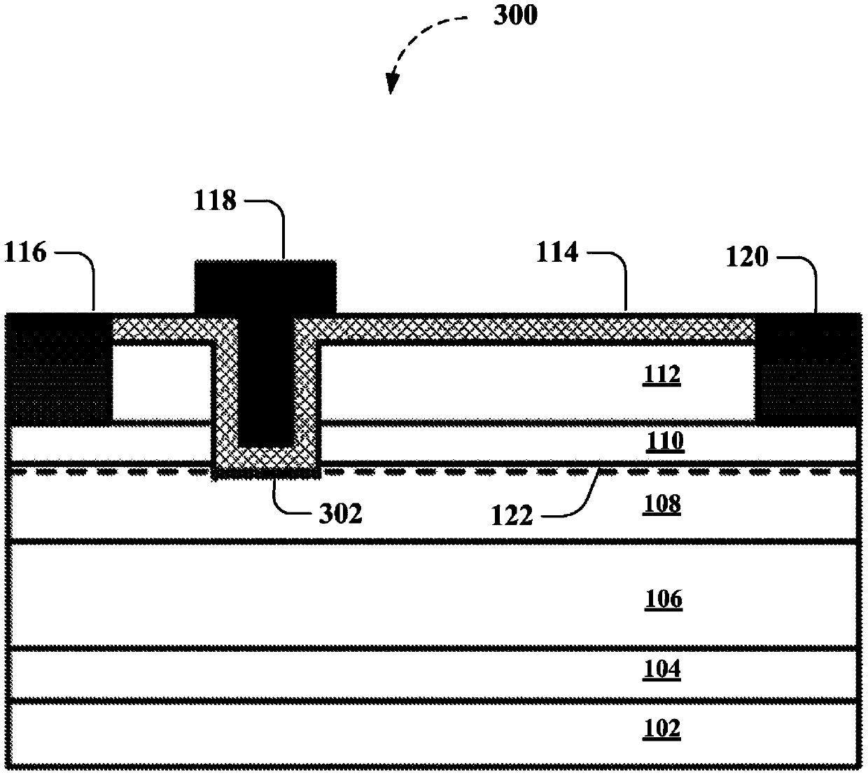
[0073] figure 2 Depicting non-limiting LPCVD-SiN according to various non-limiting aspects described herein x An exemplary cross-sectional schematic of a MIS-FET 200 including an exemplary first embodiment of a gate interfacial protective layer having an exemplary 2 nanometer (nm) plasma-enhanced chemical vapor deposition (PECVD)— SiN x Gate interface protection layer. According to various non-limiting aspects, an exemplary device 200 as described herein can include a substrate 102, a nucleation layer 104, a buffer layer 106, a semiconductor or channel layer 108, a barrier layer 110, a passivation layer 112, a gate interface protection layer 204 and gate dielectric 114 .

[0074] In a further non-limiting aspect, exemplary substrate 102 can include silicon, sapphire, diamond, SiC, AlN, GaN, and the like. Additionally, exemplary nucleation layer 104 can include AlN, GaN, InN, and / or alloys thereof, among others. In a further non-limiting aspect, the exemplary buffer laye...


PUM


Abstract

Structures, devices and methods are provided for forming an interface protection layer (204) adjacent to a fully or partially recessed gate structure (202) of a group III nitride, a metal-insulator-semiconductor high-electron-mobility transistor (MIS-HEMT) device or a metal-insulator-semiconductor field-effect transistor (MIS-FET) device, and forming a gate dielectric (114) disposed on the interface protection layer (204).

Description

[0001] Related Application Cross Reference [0002] This application claims a U.S. provisional patent entitled "INTERFACIAL PROTECTION TECHNIQUESFOR GAN POWER METAL-INSULATOR-SEMICONDUCTOR FIELD-EFFECT TRANSISTORS" filed on August 22, 2016 Priority to Application Serial No. 62 / 494813, which is hereby incorporated by reference in its entirety. technical field [0003] The subject disclosure relates to metal insulator semiconductor transistors, and more particularly, to structures, devices, and methods for creating interfacial protection layers in metal insulator semiconductor transistors. Background technique [0004] Group III nitride (III-N) compound semiconductor materials (eg, GaN, etc.) have wide energy band gap, high breakdown electric field and high thermal conductivity. In addition, typical wide-bandgap heterostructure systems (e.g., systems containing AlGaN / GaN heterostructures), enhanced by spontaneous and piezoelectric polarization effects, can generate high charg...

Claims


Application Information

Patent Timeline
Patent Type & Authority Applications(China)
IPC IPC(8): H01L29/778
CPCH01L29/4236H01L29/513H01L29/7786H01L29/2003H01L21/28264H01L29/401H01L29/66462H01L29/42356H01L29/42364
Inventor 陈敬化梦媛
Owner THE HONG KONG UNIV OF SCI & TECH
Why Eureka
Try Eureka