Method for preparing single-photon light source and component

A single-photon light source and single-photon technology, applied in electrical components, semiconductor devices, nano optics, etc., can solve the problems of low-quality single-photon light source and poor light source spectrum type, and achieve good light source spectrum type and small half-height width , high-quality effects

Active Publication Date: 2019-05-03
INST OF MICROELECTRONICS CHINESE ACAD OF SCI
View PDF5 Cites 3 Cited by
  • Summary
  • Abstract
  • Description
  • Claims
  • Application Information

AI Technical Summary

Problems solved by technology

[0003] In view of this, the purpose of the embodiments of the present invention is to provide a preparation method and components of a single-photon light source. The single-photon light source is prepared by heavy ion

Method used


Image

  • Method for preparing single-photon light source and component
  • Method for preparing single-photon light source and component
  • Method for preparing single-photon light source and component

Examples


no. 1 example

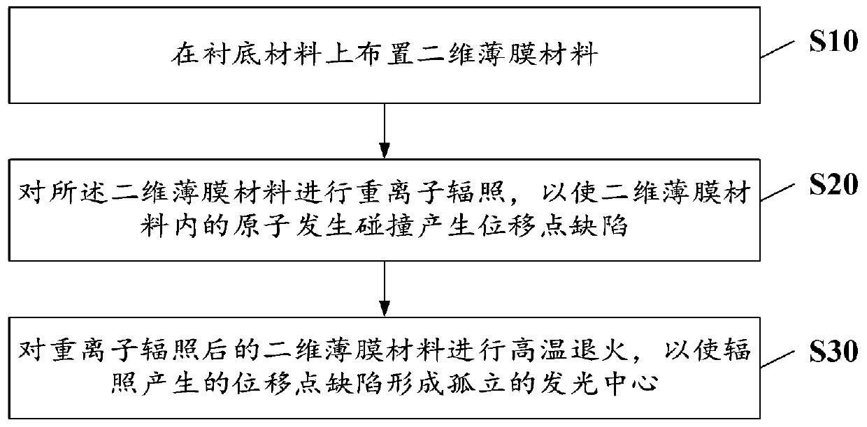
[0030] Please refer to figure 1 , figure 1 A flow chart of a method for preparing a single-photon light source provided in this embodiment is shown. The specific preparation method includes:

[0031] Step S10: Arranging a two-dimensional thin film material on the substrate material.

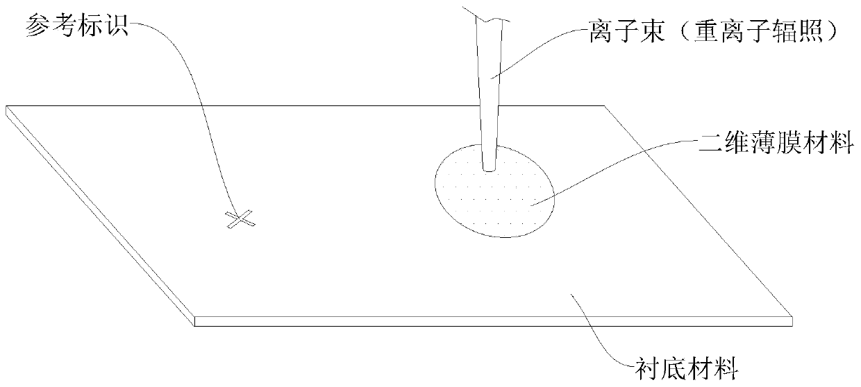
[0032] Step S20: performing heavy ion irradiation on the two-dimensional thin film material, so that atoms in the two-dimensional thin film material collide to generate displacement point defects.

[0033] Step S30: performing high-temperature annealing on the two-dimensional thin film material irradiated by heavy ions, so that the displaced point defects generated by the irradiation form isolated luminescent centers.

[0034] In step S10, the two-dimensional thin film material includes but not limited to semiconductor thin film materials such as boron nitride, gallium nitride, gallium arsenide, diamond and silicon carbide. In this embodiment, a more preferred material is a boron nitride two-...

no. 2 example

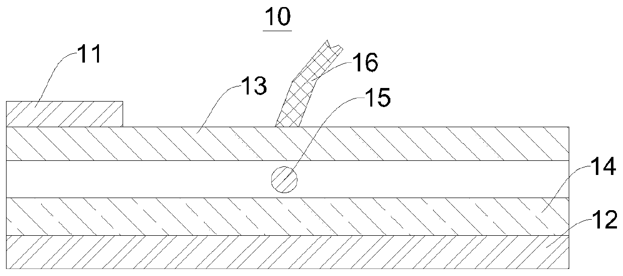
[0046] Based on the same inventive concept, the second embodiment of the present application provides a single-photon component 10 , and the single-photon light-emitting center in the single-photon component 10 can be manufactured by using the preparation method of the single-photon light source in the first embodiment. Please refer to image 3 Specifically, the single photon component 10 includes: a first electrode 11, a second electrode 12, a P-type material 13, an N-type material 14, a two-dimensional film material 15 with a single-photon emission center, and a Guided mode fiber 16 for the optical signal of the photon luminescence center; the P-type material 13 and the N-type material 14 are located on both sides of the two-dimensional thin film material 15, and the first electrode 11 is located on the P-type material 13 The side away from the two-dimensional thin film material 15, the second electrode 12 is located on the side of the N-type material 14 away from the two-di...


PUM

PropertyMeasurementUnit
Diameteraaaaaaaaaa

Abstract

The invention provides a method for preparing a single-photon light source and a component. The method comprises a step of arranging a two-dimensional film material on a substrate material, a step ofdetermining an irradiation position with the need of preparing the single-photon light source on the two-dimensional film material, a step of performing heavy ion irradiation on the irradiation position to cause collision of atoms in the two-dimensional film material to generate a displacement point defect, a step of performing high temperature annealing on the two-dimensional film material whichis subjected to heavy ion irradiation such that an isolated illuminating center is formed by the displacement point defect generated by the irradiation. The single-photon light source obtained by themethod has higher quality, the number of single photons can be effectively controlled by the heavy ion irradiation and a high temperature annealing method, the prepared single-photon light source hasgood uniformity, the light source spectrum is good, the full width at half maximum is small, and the background noise is low.

Description

technical field [0001] The invention relates to the technical field of semiconductor materials and quantum communication, in particular, to a preparation method and components of a single photon light source. Background technique [0002] With the rapid development of quantum optics and its increasingly wide range of applications, quantum information science has attracted much attention, including secure communication, quantum computing, quantum simulation, and quantum metrology. In these applications, the photon is a particularly critical physical quantum. Currently, the commonly used methods for the preparation of single photons are: 1. The single photon light source is prepared by the laser attenuation method. 2. Use the method of crystal growth to generate quantum dots in the nanometer scale in semiconductor materials. The spatially three-dimensionally confined quantum dot structure has obvious quantum confinement effects. The quantum dots form three-dimensionally confi...

Claims


Application Information

Patent Timeline
IPC IPC(8): H01L33/06H01L33/02H01L33/00B82Y20/00
Inventor 王磊李博赵发展韩郑生罗家俊刘新宇
Owner INST OF MICROELECTRONICS CHINESE ACAD OF SCI
Why Eureka
Try Eureka