Film, preparation method thereof, and QLED device

A thin film and device technology, applied in the field of thin film and its preparation, can solve the problems that the luminous efficiency of QLED devices needs to be improved, and achieve the effects of avoiding structural damage, increasing intensity, and high luminous efficiency

Active Publication Date: 2019-05-03
TCL CORPORATION
View PDF8 Cites 1 Cited by
  • Summary
  • Abstract
  • Description
  • Claims
  • Application Information

AI Technical Summary

Problems solved by technology

[0009] In view of the above deficiencies in the prior art, the purpose of the present invention is to provide a thin film and its preparat

Method used


Image

  • Film, preparation method thereof, and QLED device
  • Film, preparation method thereof, and QLED device
  • Film, preparation method thereof, and QLED device

Examples


Embodiment 1

[0077] The preparation steps of the QLED device are as follows:

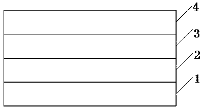
[0078] A first Cu layer of 10nm is vapor-deposited on the glass ITO substrate;

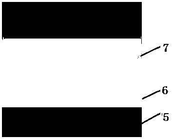
[0079] Mix 8 mg of NiO nanoparticles and 8 mg of Cu into the ethanol solution to obtain a blend solution with a concentration of 4 mg / ml, then spin-coat the blend solution on the first Cu layer, and heat it at 120 ° C for 15 min to obtain the NiO layer and the second Cu layer. A graded film with a thickness of 40nm formed by two Cu layers, in which the NiO layer is located under the second Cu layer.

[0080] Spin-coat TFB on the second Cu layer with a thickness of 10 nm;

[0081] Spin-coat QDs on the TFB layer with a thickness of 30nm;

[0082] Evaporate BCP on the QD with a thickness of 50nm,

[0083]Evaporate Al on the BCP to obtain a QLED device, the intensity of the QLED device is shown in Figure 4 .

Embodiment 2

[0085] The preparation steps of the QLED device are as follows:

[0086] Preparation of a blend solution: 4 mg of NiO nanoparticles and 6 mg of Cu were mixed into a dipropylene glycol solution with a concentration of 4 mg / ml.

[0087] After spin-coating the above blend on a glass ITO substrate, vacuum 5×10 at 70°C 2 Pa is maintained for 15min to obtain a 40nm thick gradient film formed by the NiO layer and the second Cu layer, in which the second Cu layer is located under the NiO layer; then the first Cu layer of 10nm is evaporated;

[0088] Spin-coat TFB on the first Cu layer with a thickness of 10 nm;

[0089] Spin-coat QDs on TFB with a thickness of 30nm;

[0090] Evaporate BCP on the QD with a thickness of 50nm;

[0091] Evaporate Al on the BCP to obtain a QLED device, the intensity of the QLED device is shown in Figure 4 .

Embodiment 3

[0100] The preparation steps of the QLED device are as follows:

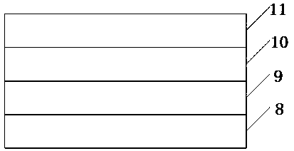
[0101] A first Cu layer of 10nm is vapor-deposited on the glass ITO substrate;

[0102] Mix 8 mg of NiO nanoparticles and 8 mg of Cu into the ethanol solution to obtain a blend solution with a concentration of 4 mg / ml, then spin-coat the blend solution on the first Cu layer, and heat it at 120 ° C for 15 min to obtain the NiO layer and the second Cu layer. A graded film with a thickness of 40nm formed by two Cu layers, in which the NiO layer is located under the second Cu layer.

[0103] Spin-coat QDs on the second Cu layer with a thickness of 30 nm;

[0104] Al is evaporated on the QDs to obtain QLED devices.


PUM


Abstract

The invention discloses a film, a preparation method thereof, and a QLED device. The film comprises a gradual change layer formed by a first metal layer, a first dielectric layer, a second dielectricand second metal which are stacked. The mass concentration of the second dielectric is gradually decreased along the thickness direction of the gradual change layer. The film has the following advantages: (1) the free electrons on the surface of the second metal interact with the photons emitted by a light-emitting layer to generate a surface plasmon propagating along the surface of the second metal, the surface plasmon may generate an electric field and resonates with an electromagnetic wave emitted by the light-emitting layer so as to enhance the light-emitting intensity and promote the composite light-emitting efficiency; and (2) a sudden change interface forms new SPE resonance having a resonance mode exactly orthogonal to the gradual change, which not only limits the diffusion of thegradual change SPE, but also provides part of the energy for the SPE so that the SPE resonance is enhanced. The film is introduced into the QLED device so as to achieve an effect of enhancing the light emission of the QLED device.

Description

technical field [0001] The invention relates to the field of QLED devices, in particular to a thin film, a preparation method thereof and a QLED device. Background technique [0002] Surface plasma enhancement (SPE) is another fascinating property of inorganic nanomaterials. For example, for coin family metals, such as silver, gold, and copper, the monomers in the nanometer size will resonate with the excitation of external electromagnetic waves of specific wavelengths to achieve the effect of enhancing the signal. The same can be applied to photoelectric conversion devices. For example, for light-emitting display diodes, the surface enhancement effect brought by nano-gold particles can be used to amplify the light emitted by semiconductor materials, thereby improving luminous efficiency. At the same time, gold nanoparticles can also be dispersed in a solvent system to facilitate subsequent processing such as spin coating, spray coating, and inkjet printing. [0003] The ...

Claims


Application Information

Patent Timeline
IPC IPC(8): H01L51/52H01L51/50H01L51/56
Inventor 向超宇邓天旸李乐张滔辛征航张东华
Owner TCL CORPORATION
Why Eureka
Try Eureka