Reverse conducting insulated gate bipolar transistor
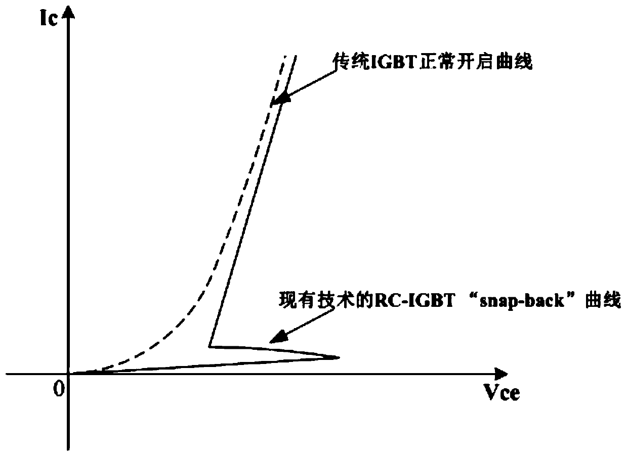
A bipolar transistor and insulated gate technology, which is applied in the field of reverse-conducting insulated-gate bipolar transistor and the structural design field of reverse-conducting insulated-gate bipolar transistor, can solve the problem of reducing the breakdown voltage of the device, burning out, and aggravating the device. problems such as non-uniformity of current distribution to achieve the effect of improving reliability
- Summary
- Abstract
- Description
- Claims
- Application Information
AI Technical Summary
Problems solved by technology
Method used
Image
Examples
Embodiment 1
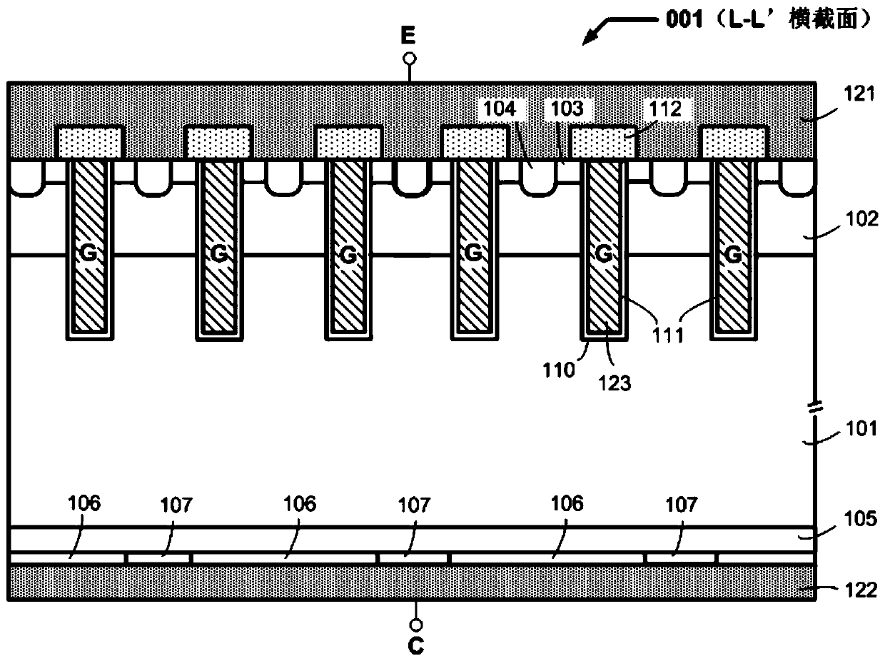
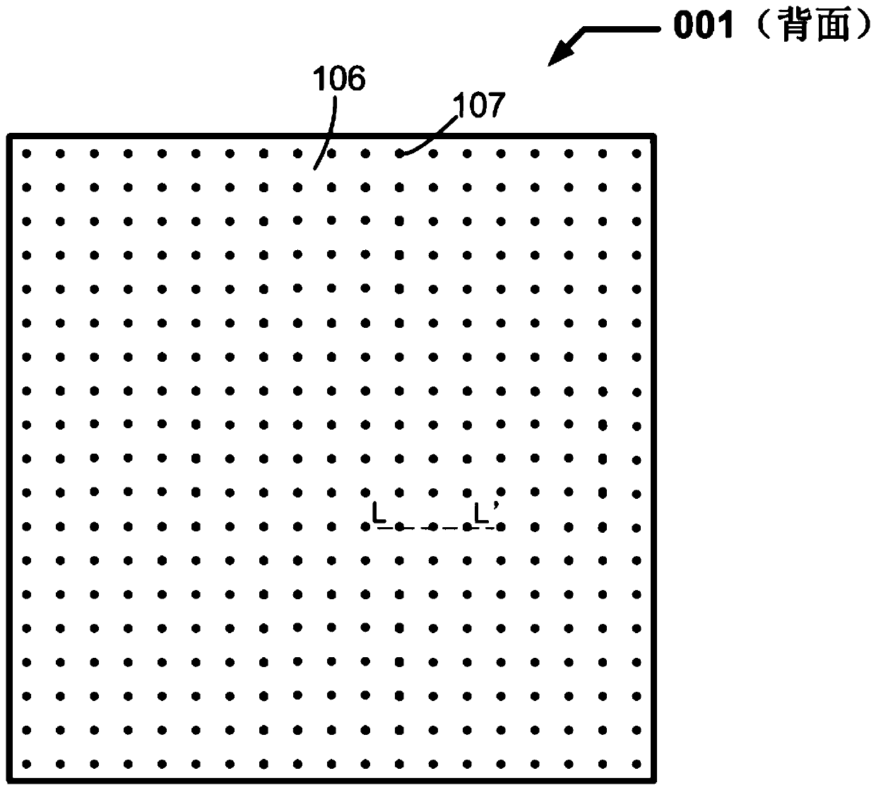
[0044] Device 002 is an RC-IGBT device according to the first embodiment of the present invention. Similar to the RC-IGBT device 001 in the prior art, the device 002 of the present invention is a trench-gate device, that is, its front side has a series of strip-shaped trenches arranged in parallel. Figure 4 It is a schematic diagram of the area division on the back of the device 002. With reference to the arrangement direction of the grooves on the front of the device, the back of the device 002 is divided into four types of rectangular areas: A, B, C, and D, wherein: Area A (21) is located on the back of the device 002 In the middle, the direction of the connection line between the center of the B district (22) and the center of the A district (21) is perpendicular to the arrangement direction of the grooves on the front of the device; The arrangement direction of grooves on the front is at an angle of 45 degrees; the direction of the connecting line between the center of th...
Embodiment 2
[0050] Figure 8 It is a schematic diagram of division of the back area of the RC-IGBT device 003 according to the second embodiment of the present invention, Figure 9It is a schematic diagram of the doping distribution of each region on the back of the device 003. Compared with the device 002 of the first embodiment of the present invention, the device 003 also has the following characteristics: there is more than one type A region (21) on the back of the device 003, and the position of the type A region (21) is not limited to the device 003 middle of the back. The region division feature of the device 003 is suitable for large-area RC-IGBT chips, which is beneficial to improving the current uniformity inside the large-area RC-IGBT chip.
Embodiment 3
[0052] Figure 10 It is a schematic diagram of division of the back area of the RC-IGBT device 004 according to the third embodiment of the present invention, Figure 11 It is a schematic diagram of the doping distribution of each region on the back of the device 004. Compared with RC-IGBT devices 002 and 003 of the present invention, device 004 also has the following characteristics: the projected area corresponding to the terminal withstand voltage region on the front of device 004 at the back of device 004 is E district (25), then E district (25 ) within n + The ratio of the cathode area is the highest, that is, δ(A)+ The cathode area (207) is fully covered without p + collector region (206). Since there is no MOS channel in the terminal withstand voltage region of the RC-IGBT, this region cannot be used as a conduction current. By increasing δ(E), p in the back region corresponding to the terminal withstand voltage region + The collector region (206) is reduced, ther...
PUM
 Abstract
Description
Claims
Application Information


