Waveguide chip for realizing nonlinear frequency conversion based on coupling waveguide

A technology for coupling waveguides and waveguide chips, which is applied in the field of wide-tuning parametric light and entangled photon source output, can solve the problems of affecting frequency conversion efficiency, unable to achieve wide-range tuning of converted light, and complexity, and achieves improved tunability and integration. High, chip-controllable effect

Active Publication Date: 2019-05-10
NAT UNIV OF DEFENSE TECH
View PDF5 Cites 8 Cited by
  • Summary
  • Abstract
  • Description
  • Claims
  • Application Information

AI Technical Summary

Problems solved by technology

Or adjust the group velocity by changing the waveguide width to achieve a wide range of phase matching, which can cover hundreds of nm[7], but at this time, filtering is required to select a specific wavelength, which will greatly affect the frequency conversion efficiency
Therefore, for the third-order nonlinear process, the frequency conversion process of a specific wavelength far away from the pumping light cannot be realized at present, let alone the wide-range tuning of the converted light.
It should be noted that the entangled photon pairs of visible light and communication light, which are far apart, have recently been realized in a silicon nitride ring waveguide cavity [8], which is achieved by carefully controlling the sidewall roughness of the ring waveguide. complex

Method used


Image

  • Waveguide chip for realizing nonlinear frequency conversion based on coupling waveguide
  • Waveguide chip for realizing nonlinear frequency conversion based on coupling waveguide
  • Waveguide chip for realizing nonlinear frequency conversion based on coupling waveguide

Examples


Embodiment 1

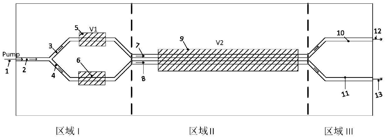
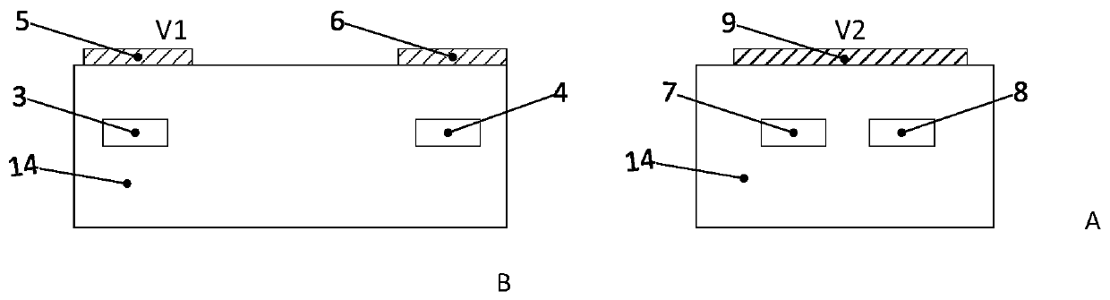
[0036] Example 1: Both the pumping light and the entangled light source are in TE mode, the wavelength of the pumping light is 1550nm, the cross-sectional size of the silicon waveguide is 500nm×220nm, the length of the waveguides 7 and 8 is 5mm, and an optical phase modulator is used on the chip to regulate the phase . figure 2 are the cross-sectional views of the thermo-optic phase modulator in region I and region II. The waveguides 3, 4, 7, 8 are surrounded by a silicon dioxide buffer layer 14. The electrodes 5 and 6 are above the waveguides 3 and 4; the electrodes 9 are both located directly above the waveguides 7 and 8. By applying a DC voltage to the electrode 5 and heating the resistance wire to change the refractive index of the silicon waveguide, the relative phases of the pumped light in the waveguides 3 and 4 are modulated to excite different modes. When a voltage of 7V is applied to the electrode 6, the relative phase of the two pumping lights changes by 2π, so t...


PUM


Abstract

The invention provides a waveguide chip for realizing nonlinear frequency conversion based on a coupling waveguide. The waveguide chip comprises: sequentially arranged pumping laser manipulation regions I, a waveguide coupling region II for generating parametric light and entangled photons, and a region III for manipulating converted light; a coupling waveguide region is arranged in a waveguide optical path region II, and the length of the coupling region should be large enough to ensure that an optical field can be coupled back and forth for multiple times; the total length of the waveguide chip is at a centimeter order; a host material of the coupling waveguide comprises various second order and third order nonlinear optical materials capable of fabricating the waveguide; a nonlinear processes occurring in the coupling region comprises all classical and quantal three-wave and four-wave action processes; the occurring nonlinear processes contain all second-order and third-order nonlinear processes, comprising frequency doubling, difference frequency, sum frequency, parametric amplification and other processes; the generated converted light contains a classical parametric light field and a quantal entangled photon source; and the waveguide chip is manipulated by using integrated thermo-optic and electro-optical effects.

Description

technical field [0001] The present invention relates to the fields of integrated optics, nonlinear optics, quantum information technology, nonlinear materials and optoelectronic technology, especially the use of integrated optics theory and technical approaches to achieve new phase matching and then realize wide tuning parametric light applicable to various waveguide materials and entangled photon source output. Background technique [0002] Phase matching is the core technology to realize frequency conversion of light field in nonlinear optics and quantum optics[1,2]. For second-order nonlinear processes, birefringence matching [3] or quasi-phase matching [4] are generally adopted. Birefringence matching is only available for anisotropic materials and requires specific angle and temperature design. Quasi-phase matching is only applicable to ferroelectric materials, and artificial high-voltage pulse electric field polarization technology needs to be introduced. For the th...

Claims


Application Information

Patent Timeline
Patent Type & Authority Applications(China)
IPC IPC(8): G02F1/35
Inventor 徐平刘英文吴超吴俊杰
Owner NAT UNIV OF DEFENSE TECH
Why Eureka
Try Eureka