Double-gate thin film transistor, sensor and manufacturing method

A thin-film transistor and sensing layer technology, which is applied in the field of electronic sensing, can solve problems affecting the integration and thinness of sensors, and achieve the effects of small size, enhanced effective voltage, and high sensitivity

Active Publication Date: 2021-01-22
BOE TECH GRP CO LTD +1
View PDF10 Cites 0 Cited by
  • Summary
  • Abstract
  • Description
  • Claims
  • Application Information

AI Technical Summary

Problems solved by technology

[0004] In view of this, the embodiment of the present invention provides a double-gate thin film transistor, a sensor and a manufacturing method, the main purpose of which is to solve the problem that most of the existing pressure sensors use thin films composed of piezoelectric materials, in order to effectively amplify the voltage of the pressure sensor. To increase the sensitivity of the signal, it is necessary to lay a large area of ​​film, and a large number of circuit traces are inserted in the film, which seriously affects the integration and lightness of the sensor as a whole.

Method used


Image

  • Double-gate thin film transistor, sensor and manufacturing method
  • Double-gate thin film transistor, sensor and manufacturing method
  • Double-gate thin film transistor, sensor and manufacturing method

Examples


Embodiment 1

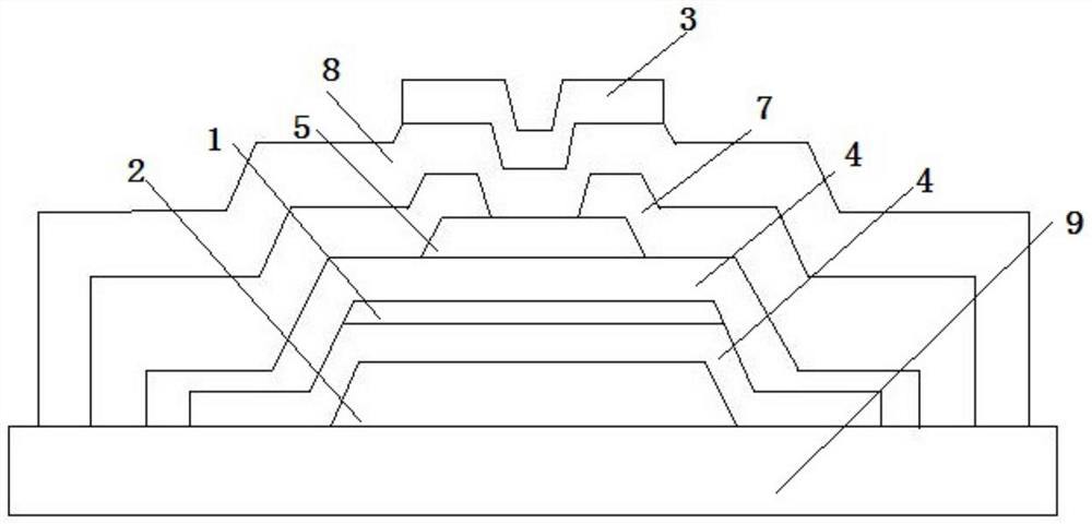
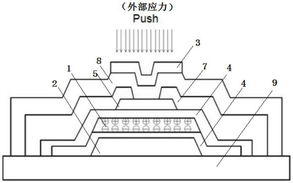
[0043] Reference attached figure 1 , the dual-gate thin film transistor provided by the embodiment of the present invention includes a stress sensing layer 1, the stress sensing layer 1 is arranged between the bottom gate 2 and the top gate 3, and the stress sensing layer 1 and A bottom gate insulating layer 4 is provided between the bottom gate 2 and the top gate 3;

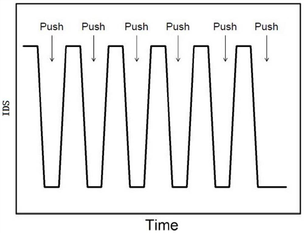
[0044] Wherein, a first preset voltage is applied to the bottom gate 2, a second preset voltage is applied to the top gate 3, the first preset voltage is greater than the second preset voltage, and the stress The sensing layer 1 forms a built-in electric field to reduce the effective gate voltage between the bottom gate 2 and the top gate 3, and the source-drain current is inversely proportional to the external pressure;

[0045] Or the first preset voltage is less than the second preset voltage, forming a built-in electric field in the stress sensing layer 1 to enhance the effective gate voltage between the bo...

Embodiment 2

[0058] Further, the embodiment of the present invention provides a double-gate thin film transistor, in a specific implementation, the stress sensing layer 1 includes a plurality of stress sensing units;

[0059] The stress sensing unit includes a piezoelectric material and a bottom gate insulating layer 4, and the bottom gate insulating layer 4 is respectively provided at the upper and lower ends of the piezoelectric material;

[0060] Wherein, the plurality of stress sensing units are stacked.

[0061] Specifically, in order to improve the sensitivity of the double-gate thin film transistor, in the technical solution adopted by the present invention, the stress sensing layer 1 is designed with a multi-layer structure, that is, the bottom gate insulating layer 4, the piezoelectric material, the bottom gate The insulating layer 4 is one layer, and the same structure is stacked in multiple layers, and both ends must be bottom gate insulating layers 4; two layers of bottom gate ...

Embodiment 3

[0066] Further, refer to the attached Figure 5 The method for manufacturing the double-gate thin film transistor described in the foregoing embodiments provided by the embodiments of the present invention includes the following steps:

[0067] S1, cleaning the substrate 9;

[0068] S2. Prepare the bottom gate 2 on the substrate 9 and perform patterning treatment on it. The material for making the bottom gate 2 can be metal conductive material and oxide conductive material;

[0069] S3. Prepare a bottom gate insulating layer 4 on the bottom gate 2, and pattern it. The material for making the bottom gate insulating layer 4 can be silicon nitride (SiN x ), alumina (Al 2 o 3 ) and silicon dioxide (SiO 2 ) and other insulating materials;

[0070] S4. Prepare a stress sensing layer 1 on the bottom gate insulating layer 4, and perform patterning on it. The orthographic projection of the stress sensing layer 1 should at least coincide with the bottom gate 2, so The stress sensi...


PUM


Abstract

The invention discloses a dual-gate film transistor, a sensor and a manufacture method, relating to the technical field of electronic sensing. The dual-gate film transistor comprises a stress sensinglayer, wherein the stress sensing layer is arranged between a bottom gate electrode and a top gate electrode, bottom gate electrode insulating layers are respectively arranged between the stress sensing layer and the bottom gate electrode and between the stress sensing layer and the top gate electrode, a first preset voltage is applied to the bottom gate electrode, a second preset voltage is applied to the top gate electrode, the first preset voltage is greater than the second preset voltage, a built-in electric field is formed in the stress sensing layer so as to lower effective gate electrode voltage between the bottom gate electrode and the top gate electrode, and a source leakage current and an external pressure are in inverse ratio; or the first preset voltage is less than the secondpreset voltage, the built-in electric field is formed in the stress sensing layer so as to enhance effective gate electrode voltage between the bottom gate electrode and the top gate electrode, and the source leakage current and the external pressure are in direct ratio.

Description

technical field [0001] The invention relates to the technical field of electronic sensing, in particular to a double-gate thin film transistor, a sensor and a manufacturing method. Background technique [0002] A sensor is a detection device that can feel the measured information, and can transform the sensed information into electrical signals or other required forms of information output according to certain rules, so as to meet the needs of information output, processing, storage, display, Recording and control requirements; Since the 21st century, sensors have become more and more widely used in smart medical care. The connection between sensors and human health is to detect the release of human mechanical energy, such as breathing, heartbeat, blood flow and lung expansion / contraction, etc. , to effectively convert mechanical energy into electrical signals; technologies for detecting mechanical energy include piezoelectric effect, triboelectric effect, magnetostrictive e...

Claims


Application Information

Patent Timeline
Patent Type & Authority Patents(China)
IPC IPC(8): G01L1/16G01L9/08H01L29/786H01L21/336
Inventor 曾勇陈周煜林滨付婉霞乐发垫霍亚洲王洋
Owner BOE TECH GRP CO LTD
Why Eureka
Try Eureka